

диафрагмированные волноводные фильтры / 6a3b4170-bd72-4ab1-8170-bb99dbdbc4e5
.pdfThis article has been accepted for publication in a future issue of this journal, but has not been fully edited. Content may change prior to final publication. Citation information: DOI 10.1109/TASC.2017.2654350, IEEE Transactions on Applied Superconductivity
4EPo1B-05 |
1 |
Novel Design of Band-Pass Waveguide Filter with HTS E-Plane Insert
Yu-Sheng He, Alexander Barannik, Member, IEEE, Nickolay Cherpak, Senior Member, IEEE, Liang Sun, Valerii Skresanov, Yongbo Bian, Jia Wang, Mikhail Natarov, and Vladimir Zolotaryov
Abstract— In this paper, the idea of a band-pass filter (BPF) with HTS E-plane insert in the cross waveguide is implemented in Ka-band. The advantage of this approach is to solve the problem of mounting HTS insert into the body of the metal waveguide in order to ensure good electrical contact. A three-step method for the synthesis and design of such a filter is proposed and implemented. The method includes synthesis of the normalized prototype filter, sequentially iterative synthesis of filter geometry and the final synthesis with optimization using numerical electrodynamic analysis of the entire geometry. It is shown that for the narrowband BPF, resonance windows in the E-plane insert should be performed with accuracy better than ±0.2 m. The characteristics of such filters are expected better or not worse than their counterparts on the basis of rectangular waveguides, but at less stringent conditions of fastening HTS insert in body of the waveguide. For fabricating the BPF, epitaxial HTS YBa2Cu3O7- films sputtered on both sides of MgO single crystal dielectric substrate of 0.5 mm thickness were used. The difference between losses in the produced filter and its simulated sample is explained with insufficient accuracy of making resonance windows in the HTS insert.
Index Terms—microwave filters, millimeter wave circuits, surface impedance, superconducting microwave devices.
I. INTRODUCTION
FILTERS are specific devices, which are used in many microwave systems. Their role is to separate or confine microwave frequencies. Modern applications e.g. wireless communications, radar systems and radio astronomy need microwave filters with increasingly high performance. As practically all microwave devices, filters can be fabricated on
the basis of different transmission lines [1].
The advance of high-temperature superconductor (HTS) had resulted in tremendous number of new microstrip and other filters [1], [2]. However, until now works on HTS filters on the basis of hollow waveguides are extremely scanty. The idea to create a band-pass filter (BPF) with HTS E-plane insert in rectangular waveguide was proposed and discussed in [3]. After then, the approach to designing the filter was used in [4].
Corresponding author: Liang Sun.
L. Sun (e-mail: sunliang@iphy.ac.cn), Y. S. He (e-mail: yshe@aphy.iphy.a c.cn), Y. Bian (e-mail: bianyongbo@iphy.ac.cn), and J. Wang (wangjia@iphy. ac.cn) are with the Institute of Physics, Chinese Academy of Sciences, Beijing, 100190 China.
A. Barannik (e-mail: a.a.barannik@mail.ru), N. Cherpak (e-mail: cherpak@ire.kharkov.ua), V. Skresanov (e-mail: skresanov@ire.kharkov.ua), M. Natarov (e-mail: m.nataroff@gmail.com) and V. Zolotaryov (e-mail: greenlight057@gmail.com) are with O. Ya. Usikov Institute for Radiophysics and Electronics of National Academy of Sciences of Ukraine, Kharkiv, 61085 Ukraine.
However the ways to fabricate HTS-based waveguide filters, which were seemed perspective in millimeter wavelength range, remained under question.
A new approach to fabricate the BPF in Ka-band with bilateral HTS E-plane insert in the rectangular waveguide was made in [5]. Result of this work shown that, from point of view of the gain in reducing insertion losses, fabricating the narrow BPF is expedient. However at the same time a serious technical problem arises. The problem is conditioned by necessity of both good electric and thermal contact between HTS E-plane insert and halves of waveguide housing. The authors of [5] faced with frequent breakdowns and cracking of inserts, i.e. dielectric substrates with HTS structure.
It has become clear that we need new idea to design the waveguide filters. Such an idea became a concept of patent [6], where authors proposed to change distribution of microwave field in waveguide cross-section with the purpose to decrease field intensity and hence microwave current density in place of abovementioned contact. For solving this problem authors [6] proposed to use cross waveguide (CWG) instead of rectangular one. CWG presents a result of evolution of rectangular waveguide, in which rectangular grooves are made in wide walls of rectangular waveguide. Preliminary results of design, simulation and some testing of the CWG-based BPF were reported in [7].
In this paper we present more complete results obtained on simulation and experimental study of BPF with HTS E-plane insert in CWG.
II. GENERAL STRUCTURE OF FILTER AND RESULTS OF
SIMULATION
A. Comparison of Two Waveguide Structures
Designs of BPFs with HTS E-plane insert in rectangular and CWG are presented in Fig.1a and Fig.1b accordingly. The main obvious difference in the structures of these filters is the presence of the grooves in the broad walls of CWG. Width values of narrow and wide walls of the input and output rectangular waveguides are equal to dimensions a and b of CWG (see below, Fig. 4a). The width of the grooves must be significantly greater than the thickness of HTS inserts. The width and depth of the grooves are optimized in order to minimize the losses in the contact region, since the microwave field distribution in a cross-section of the waveguide changes.
Other, less obvious, differences is listed below in presenting the experimental results of the study of prototype filter. The simulation of MW currents for the two types of BPFs shows that current density in a place of fixing HTS E-plane insert is
1051-8223 (c) 2016 IEEE. Personal use is permitted, but republication/redistribution requires IEEE permission. See http://www.ieee.org/publications_standards/publications/rights/index.html for more information.

This article has been accepted for publication in a future issue of this journal, but has not been fully edited. Content may change prior to final publication. Citation information: DOI 10.1109/TASC.2017.2654350, IEEE Transactions on Applied Superconductivity
4EPo1B-05
a)
b) |
c) |
d)
Fig.1. Photoes of BPFs with HTS insert in: (a) rectangular waveguide [5] and
(b) CWG, and (c) perspective view of BPF based on CWG [7] with (d) HTS insert; 1-CWG, 2-single crystal dielectric substrate, 3-HTS film structure, 4- resonator, 6-waveguide body (two parts) of the filter.
much smaller in the CWG [7].
B. Synthesis Problem of BPF with E-plane Insert in Cross Waveguide
The proposed filter has a complicated geometry and contains materials with different electrophysical properties, so the filter synthesis was carried out without using rigorous electrodynamic analysis of the whole structure. The authors resorted to, so to speak, the hybrid method of filter synthesis. This method includes three steps of design:
Synthesis of the normalized prototype filter;
Sequentially iterative synthesis of filter geometry;
The final synthesis with optimization using numerical electrodynamic analysis of the entire geometry.
We designed a 5-pole filter of the bandwidth BW≈140 МHz and a center frequency 30.5 GHz.
Filter simulation begins with the calculation of so-called normalized prototype filter. The prototype contains the information necessary for the following steps of the synthesis of microwave filter, i.e. the required number of resonators (filter order), their resonant frequencies, mutual coupling coefficients and the values of external Q-factor [8]. We obtained the external Q-factor QEX= 230.7 and the coefficients
of mutual coupling K1,2= K4,5=0.0033, K2,3= K3,4=0.0032 between the neighboring resonators, where 1, …, 5 are
numbers of the resonators [7].
In the second step we synthesize the filter geometry. In this step, the whole geometry is divided into elements, which consist of separate pairs of coupled resonators formed by the windows in the E-plane insert with the surrounding walls of the waveguide. The calculation of the S-matrix of individual resonators is performed numerically using CST Microwave Studio program product for electrodynamic simulation. First of all simulation of BPF with perfect conducting insert was
2
Fig. 2. Simulated response of filter after optimization steps.
carried out using System of Electromagnetic Simulation (MWD II) developed at Institute for Radiophysics and Electronics of NAS of Ukraine (IRE NASU). Further the program product CST Microwave Studio was used for calculation taking into account final conductivity of E-plane insert (see Fig. 3 in [7]). The results showed their good correspondence for rectangular waveguide-based BPF. Therefore this approach was used for simulation of CWG BPF also.
The second step is to iteratively adjust the geometry of the coupled resonators to achieve the parameters obtained in the first step of the design for each pair of resonators. Detail is as follows: one of the coefficients, namely S21 transmission or S11 reflection, is chosen. Then this ratio is subjected to linearfractional approximation by means of the computer program (Shaman) composed at IRE NASU [9].
After this procedure, a series of parametric vectors are derived automatically from the frequency response of coefficients: the amplitude of the resonance oscillations (modes), phases, Q-factors, and eigen frequencies. To achieve the required filter response given in the first step, we need to get the parameter vectors in accordance with the prototype low-pass filter parameters.
The final step is introduced in order to achieve the performance identity of the filter, synthesized in the second step and calculated in the first step. We resort to optimization by means of numerical electrodynamic analysis to eliminate inconsistencies. The goal of optimization is the attainment of a given level of return loss in the first step. With the reduction of the bandwidth, the influence of geometrical dimensions on the filter response increases dramatically. This imposes a requirement to comply with values of the parametric vectors obtained for a prototype as closely as possible. According to the proposed method, it is not possible to configure narrowband filter in one "iteration" step because we have the limited resources in computer operating using the inherent model in CST Microwave Studio. As a consequence, distortion of filter frequency response is observed after assembling of the entire structure. Moreover, the presence of loss in the filter elements distorts also the response of the filter, since the calculation of loss in the prototype model is not laid. The optimization algorithms embedded within the CST was used (Fig.2).
1051-8223 (c) 2016 IEEE. Personal use is permitted, but republication/redistribution requires IEEE permission. See http://www.ieee.org/publications_standards/publications/rights/index.html for more information.
This article has been accepted for publication in a future issue of this journal, but has not been fully edited. Content may change prior to final publication. Citation information: DOI 10.1109/TASC.2017.2654350, IEEE Transactions on Applied Superconductivity
4EPo1B-05 |
3 |
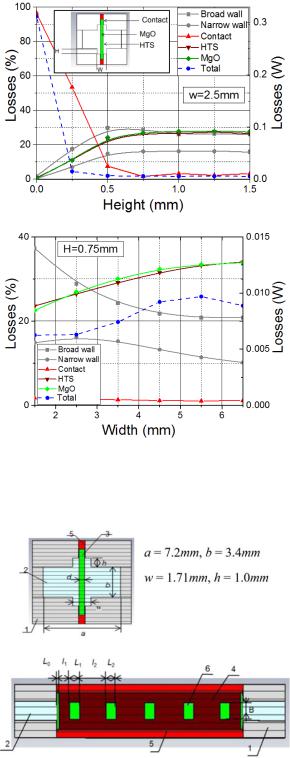
Ka-band, losses in the contact area decreases noticeably at increase of H up to ~ 0.75mm. At the same time, they are independent practically on w.
"Iterative" step gives a very good first approximation for optimization, which is very significantly reduces the time and the number of iterations to achieve the objectives, in this case, the level of return loss.
At the same time, simulation shows that production of the proposed filter will meet the technological problem, which is conditioned with achieving submicrometer accuracy of making E-insert resonant windows [7].
III. EXPERIMENTAL DETAILS AND RESULTS
a)
b)
Fig. 3. Dependence of relative losses in separate elements of filter on (a) height H and (b) width w of groove in broad wall of CWG when total losses are 100% for each H or w values. Fig. 3a and Fig. 3b show also total absolute losses (dashed lines), which are calculated for the input power of 1 W. Inset in Fig. 3a shows a cross-section of the BPF.
a)
b)
Fig.4. (a) Cross-section and (b) view of HTS E-plane insert housed in CWG, when a front half of CWG body is removed; 1-WG body, 2-WG channel, 3- dielectric substrate, 4-HTS film, 5-area of contact of HTS film and CWG body; 6-resonant windows in HTS film 4 sputtered on substrate 3.
C. Simulation Consequences
Results of simulation show dependence of microwave energy loss in CWG depending on depth H and width w of groove in broad wall waveguide (Fig.3). One can see that, for
A. Experimental Details
Epitaxial HTS YBa2Cu33O7- films sputtered on both sides of MgO single crystal dielectric substrate of 0.5 mm thickness was used to make an experimental prototype of the filter. The characteristics of the film were as follows: thickness was 600 nm and Tc was about 90 K. The films were produced by company Ceraco.
E-plane insert is a plate of dielectric substrate coated on both sides with identical HTS-based structures made by photolithography with accuracy of ± 1-2 m. The structures represented the sequence of resonant "windows" disposed at a certain distance from each other and from the edges of the insert.
The E-insert is placed between halves of CWG body, which was made of brass covered with silver layer of ~ 1 m (Fig. 4).
There were technological clearances (gaps) of ~ 100 m thickness between the insert and waveguide body for the purpose of placing the pressure plate of phosphor bronze.
The measurements were carried out in a cryogenic chamber, which allows achieving temperature 64 K using liquid nitrogen. The frequency response of the filter was measured by means of the hardware-calculating system for measurement of high-Q resonator characteristics at the frequency range from 26 GHz to 37.5 GHz [10].The system was tested using Network Analyzer PNA-L N5230A.
B. Experimental results and Discussion
Measurement results of the 5-pole BPF frequency response are given in Fig.5. Insertion loss (S21) can reach to ~ - 1.2 dB in a center of pass-band and lower than loss with the cooled copper insert (Fig. 5b). At the same time, the measured S21 in pass-band has noticeable difference from simulated one especially at the band edges. The frequency band of the measured return loss (S11) better than -17 dB level is about half of that of the simulated S11 (Fig. 2b) and has no deep dips in S11 vs. frequency in Fig. 5(a). In addition, the lowfrequency part of the measured S21 is higher than the simulated
S21.
Though the measured performance of the filter confirms the simulation results, the deviations indicate that it is necessary to keep the accuracy of manufacturing resonant windows in the insert within the limits of ± 0.2 m when fabricating narrowband filters with HTS E-plane insert [7].
1051-8223 (c) 2016 IEEE. Personal use is permitted, but republication/redistribution requires IEEE permission. See http://www.ieee.org/publications_standards/publications/rights/index.html for more information.

This article has been accepted for publication in a future issue of this journal, but has not been fully edited. Content may change prior to final publication. Citation information: DOI 10.1109/TASC.2017.2654350, IEEE Transactions on Applied Superconductivity
4EPo1B-05 |
4 |
a)
b)
Fig.5. Frequency response of 5-pole BPF with HTS E-plane insert in the CWG: (a) experimental and simulated data on the insertion loss (S12) and return loss (S11), the calculated central frequency is shifted, (b) an insertion loss (S12) in an enlarged scale at comparing with losses with Cu insert at 78K ( blue) and 295 K (black) in rectangular waveguide.
Fig. 6. Changing values of S11 at two frequencies (see S11 in Fig. 2 depending on variation of the length L3 of central resonant window (see Fig. 4b).
Tolerances on keeping the length of the resonators play a decisive role in the response of the filter. Fig. 6 presents changing maximum values of S11 at two frequencies (f=30.45GHz and 30.49GHz in Fig. 2) depending on variation of the central window length L3 (see Fig. 4b). Design characteristics can be achieved if the length is sustained with accuracy ± 0.2 μm. Such dependence is the most strong only
for window size because it determines resonant frequency. For this reason, the dependence of S-parameters on the small (±1
μm) both the variation of distance between the windows and the relative displacement of the window patterns on opposite sides of the substrate is substantially weaker concerning S11 parameter. At the same time the central frequency shifts in the latter case (e.g. 18 MHz at 0.2 μm displacement).
The effect of displacement of the substrate with HTS structures in a transverse cross-section of the CWG will be studied elsewhere.
IV. CONCLUSION
To summarize, the work shows the possibility of design and fabricating a narrow-band filter with HTS E-plane insert in the CWG. The filter has the following advantages: (i) reduction ofthe requirements for electric contact between the HTS insert and metal waveguide housing and (ii) the ability to increase operating frequency, at least up to the K-band. However, the manufacture of the filter requires a rather high precision of making the resonant windows in HTS insert, namely in the Ka-band within ±0.2 m. The work confirms the earlier conclusion about the prospects of raising the operating frequency in the HTS-based passive microwave devices up to Ka-band [11].
REFERENCES
[1]Jia-Sheng Hong, and M. J. Lancaster, Microstrip Filters for RF / Microwave Applications, John Wiley & Sons, Inc, USA: 2001.
[2]L. Sun, and Y. He, “Research progress of high temperature superconducting filters in China,” IEEE Trans. Appl. Supercond.,vol. 24, no. 5, October 2014, Art. 1501308.
[3]R. R. Mansour, A. Zybura, “Superconducting Millimeter-Wave E-Plane
Filters,” IEEE Trans. Microwave Theory Tech., vol.39, pp. 1588-1492, September 1991.
[4]L. Han, Y. Chen, Y. Wang, Q. Cheng, S. Yang and P. Wu, “Design and
Performance of Waveguide E-Plane HTSC Insert Filters,” IEEE IMSDigest, IF2 1-4, pp. 912-916, 1992.
[5]V. N. Skresanov, A. A. Barannik, N. T. Cherpak, Y. He, V. V. Glamazdin, V. A. Zolotaryov, A. I. Shubny, L. Sun, J. Wang, Y. Wu,
“Experience in developing Ka-band waveguide filter with HTS E-plane insert,” The 8th International Kharkiv Symposium MSMW, Kharkiv. Ukraine, p.661-663, 2013.
[6]V.N. Skresanov, A.A. Barannik, V.V. Glamazdin, V.A. Zolotaryov, M. P. Natarov N. T. Cherpak, A. I. Shubny, Yusheng He, Liang Sun, Jia Wang, Xu Wang, Yun Wu, “Band-Pass Filter,” Patent № 109490, Ukraine, 25 August 2015.
[7]V. A. Skresanov, A.A.Barannik, N. T. Cherpak, V. V. Glamazdin, A. I. Shubny, Y. S. He, L. Sun, “Elecrodynamic Features and Design of Filter
Based on HTS E-plane Insert in a Cross Waveguide”, The 9th International Kharkiv Symposium MSMW, Kharkiv, Ukraine, June 2016.
[8]J. L. Matthaei, L. Young, E. M. T. Jones, Microwave Filters, Impedance-Matching Networks, and Coupling Structures, New York, USA: McGraw-Hill Co., 1968.
[9]V. N. Skresanov, V. V. Glamazdin, N. T. Cherpak, “The Novel Approach to Coupled Mode Parameters Recovery from Microwave
Resonator Amplitude Frequency Response,” Proceedings of the 41st European Microwave Conference (EuMC 2011), 10-13 October 2011, Manchester, UK, p. 726-729, 2011.
[10]V. N. Skresanov, V.V. Glamazdin, A.I. Shubny, Z.Ye. Eremenko,
“Hardware computing system for measurement of low and high quality resonators characteristics within the frequency bandwidth from 26 GHz to 37.5 GHz”, Telecommunications and Radio Engineering, vol.70, no.7, p.25-647, 2011.
[11]N.T.Cherpak, “High-temperature superconductors and MM wave technology: challenge and perspectives,” The 5th International Kharkiv Symposium MSMW, Kharkiv, Ukraine, vol. 1, p.412-414, June 2004.
1051-8223 (c) 2016 IEEE. Personal use is permitted, but republication/redistribution requires IEEE permission. See http://www.ieee.org/publications_standards/publications/rights/index.html for more information.