

диафрагмированные волноводные фильтры / ac46c243-d595-4726-ab12-49f0b18c4817
.pdfHalf Mode Substrate-Integrated Waveguide-Loaded
Evanescent-Mode Bandpass Filter
Lee W. Cross, Mohammad J. Almalkawi, Vijay K. Devabhaktuni
EECS Department, The University of Toledo, 2801 W. Bancroft Street, Toledo, OH
Received 5 December 2011; accepted 12 April 2012
ABSTRACT: In this article, a filter size reduction of 46% is achieved by reducing a substrate-integrated waveguide (SIW)-loaded evanescent-mode bandpass filter to a halfmode SIW (HMSIW) structure. SIW and HMSIW filters with 1.7 GHz center frequency and 0.2 GHz bandwidth were designed and implemented. Simulation and measurements of the proposed filters utilizing combline resonators have served to prove the underlying principles. SIW and HMSIW filter cavity areas are 11.4 and 6.2 cm2, respectively.
Wiley Periodicals, Inc. Int J RF and Microwave CAE 00:000–000, 2012.
Keywords: bandpass filter; combline; half-mode substrate integrated waveguide (HMSIW); loaded evanescent-mode cavity
I. INTRODUCTION
Microwave filters are integral components in systems for wireless communication, audio and video broadcast, radar, power transmission, imaging, and sensors. Design and miniaturization of microwave filters is an ongoing research topic where filters are designed for specified performance such as bandwidth, insertion loss, and spurious-free range, while minimizing size, weight, and fabrication cost. Highperformance narrow-band microwave filters have traditionally been implemented in air-filled waveguide form with attendant large size, high weight, and costly fabrication [1]. Waveguide structures have been fabricated in planar form using printed circuit board (PCB) manufacturing processes to form dielectric-loaded substrate-integrated waveguides (SIWs) that reduce size, maintain waveguide performance, and are as easily fabricated as planar microwave filters [2].
Conventional SIW filters can further reduce size up to 50% by cutting the structure in half along the E-plane to form the half-mode SIW (HMSIW) structure [3–5]. Conventional HMSIW structures have low radiation loss, provided they are operated above cutoff, limiting usefulness in compact lowfrequency microwave filters [6]. Waveguide components such as directional filters and couplers can be readily implemented with this transmission line structure [7, 8].
Loading the SIW cavity with capacitive posts allows operation below cutoff, reducing filter size and offering
excellent spurious-free range characteristic of evanescentmode filters [9]. Ridge SIW and folded SIW filters offer size reduction beyond SIW and HMSIW filters when capacitively loaded to operate in evanescent mode [10]. Evanescent-mode resonators may be fabricated in substrates using many configurations of cavities and capacitive loading to allow considerable design flexibility [11]. Substrate-integrated filters including bandpass and band- pass–bandstop have been constructed by coupling a series of cavities, each with a single evanescent-mode resonator per cavity [12, 13]. Reconfigurable filters and di-, tri-, and multiplexers have been made in this form [14, 15].
This article presents an evanescent-mode SIW combline bandpass filter where a cavity is loaded with capacitive posts, and then further size reduction is demonstrated by cutting the structure in half to form an HMSIW filter. This structure is a novel combination of both half-mode and evanescent-mode operation that reduces size while preserving filter performance.
This article is organized as follows: Section II presents the design of third-order filters in evanescent-mode SIW and HMSIW form. Section III presents simulation model and measured filter S-parameter results and compares filter size with conventional SIW resonators. Section IV summarizes the work and conclusions.
II. FILTER DESIGN
Correspondence to: |
V. |
K. Devabhaktuni; e-mail: |
vijay. |
A. Filter Prototype |
devabhaktuni@utoledo.edu) |
|
|
||
|
|
The third-order bandpass filter prototype shown in Figure 1 |
||
DOI 10.1002/mmce.20662 |
|
|
||
|
|
is a symmetric structure in which component values and |
||
Published online in |
Wiley |
Online Library |
|
|
(wileyonlinelibrary.com). |
|
|
mechanical dimensions are mirrored about the center |
|
VC 2012 Wiley Periodicals, Inc.
1
2 Cross, Almalkawi, and Devabhaktuni
Figure 1 Symmetrical filter prototype with three coupled resonators and inductively coupled ports.
resonator, which reduces modeling and optimization effort. The topology is easily implemented in evanescentmode SIW and HMSIW form.
The resonators have identical capacitance and resonant frequency. Inter-resonator elements L2 control bandwidth, and L1 sets port coupling.
The filter specification used in this article is center frequency and bandwidth of 1.7 and 0.2 GHz, respectively, and return loss of <15 dB. The ideal filter model with lumped element values in Table I achieves this specification.
B. Physical Structure
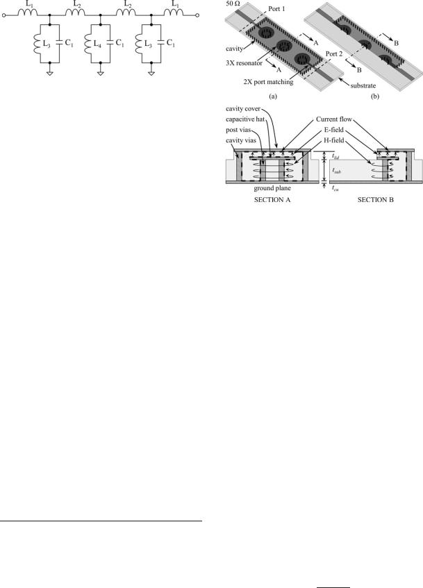
The prototype filter is implemented in SIW and HMSIW form as rectangular cavities loaded with inline posts. Ports 1 and 2 are driven with 50 X microstrip transmission lines. High-impedance port matching lines direct couple outer resonators with L1. Inter-resonator magnetic coupling is realized with L2. Resonator posts are heavily loaded with C1 to decrease operating frequency. SIW posts are approximated with ten-via circular arrays, and HMSIW posts are five-via semicircles. The SIW cavity in Figure 2a consists of a ground plane defining the bottom, regularly spaced vias for sides, and a thin lid layer on top bonded to the substrate. Each post and surrounding cavity defines resonator inductors L3 and L4.
The HMSIW filter in Figure 2b consists of the SIW cavity cut in half along the E-plane (feed line) axis, exposing the centerline of the cavity and posts. Edges of the feed and matching lines are aligned with the centerline. In this way, filter area is reduced by half. Parameters of the HMSIW filter are adjusted to achieve identical filter performance.
E-field at capacitive hats is shown by vertical vectors in sections of Figure 2. H-field around resonator posts is shown with horizontal circular vectors. Current flows at
TABLE I Ideal Model Values for Proposed SIW and HMSIW Filters
Lumped |
|
SIW |
HMSIW |
Element |
Description |
Value |
Value |
|
|
|
|
C1 |
Resonator capacitance |
16.93 pF |
8.47 pF |
L1 |
Port coupling |
3.0 nH |
6.2 nH |
L2 |
Inter-resonator coupling |
6.8 nH |
13.5 nH |
L3 |
Outer resonator inductance |
0.591 nH |
1.261 nH |
L4 |
Inner resonator inductance |
0.608 nH |
1.217 nH |
|
|
|
|
Figure 2 (a) SIW and (b) HMSIW filter implementations showing cavity structure, port matching lines, and resonators integrated into substrate. Sections A and B show resonator post E-field and H-field lines.
the surface of the conductors inside the cavity along the path defined by the dashed lines.
III. FILTER IMPLEMENTATION
The filters are designed for readily available Rogers 4003C materials of base substrate layer thickness, tsub, of 1.524 mm and lid layer thickness, tlid, of 0.203 mm. The selected lid layer material is the thinnest laminate that may be bonded to the outer layer of a PCB stackup. Relative dielectric constant, er, used for simulations is 3.55. Dielectric loss tangent, df, is 0.0021, which sets an upper limit for resonator quality factor. Copper thickness, tcu, is 35 lm (weight, 1 oz). Microstrip width is 3.35 mm to achieve 50 X impedance. Filter models were optimized and simulated in Ansys HFSS.
A. Filter Optimization
Filter geometry was optimized to achieve specified performance with as many similar measurements as possible to facilitate area comparison. Cavity width is set to 20 and 10 mm for SIW and HMSIW filters, respectively. Dimensions shown in Figure 3 and Table II achieve identical filter response and similar cavity length, L.
The HMSIW filter requires smaller post radii R1 and R2 to maintain equal center frequency. Weaker port and inter-resonator coupling are realized with higher impedance matching lines (reduced Mw) and longer inter-resona- tor spacing, S.
Capacitive hats are fixed diameter, D, with C1 calculated from the following equation.
e0erp D 2
C1 ¼ 2 (1)
tlid
International Journal of RF and Microwave Computer-Aided Engineering/Vol. 000, No. 000, Month 2012

HMSIW-Loaded Evanescent-Mode BPF |
3 |
Figure 3 Physical dimensions of (a) SIW and (b) HMSIW filters.
The values are found to be 16.93 pF for SIW and 8.47 pF for HMSIW posts neglecting fringing capacitance. Resonator inductance is the equivalent inductance of a shorted coaxial transmission line with the center profile of the circular via array and outer profile of the cavity [16]. Characteristic impedance of the irregular shape need not be directly computed; the post via array radius is simply adjusted to tune each resonator. Passband center frequency is determined by hat capacitance in conjunction with resonator inductance, and is set to 1.7 GHz by selecting appropriate values for D and tsub, respectively.
Filter substrates shown in Figure 4 are fabricated using standard two-layer PCB processing and impedance control for 610% transmission line tolerance. Lid layers were fabricated from single-sided laminate and attached to substrates with short wires soldered through each via barrel connecting top and bottom. Filters use SMA edge connectors.
IV. RESULTS AND DISCUSSION
The proposed filters were measured with a Rohde & Schwarz ZVB20 VNA with TRL calibration. The air gap
TABLE II Dimensions of Proposed SIW and HMSIW
Filters
|
|
|
HMSIW |
Lumped |
|
SIW Value |
Value |
Element |
Description |
(mm) |
(mm) |
|
|
|
|
L |
Cavity length |
57.20 |
62.20 |
W |
Cavity width |
20.00 |
10.00 |
S |
Resonator spacing |
18.60 |
21.10 |
R1 |
Outer postradius |
2.82 |
1.98 |
R2 |
Inner postradius |
2.90 |
2.50 |
Mw |
Matching line width |
2.50 |
0.50 |
Ml |
Matching line length |
8.00 |
D |
Posthat diameter |
11.80 |
tlid |
Lid layer thickness |
0.203 |
tsub |
Substrate thickness |
1.524 |
tcu |
Copper thickness |
0.035 |
Figure 4 Photographs of the evanescent-mode SIW and HMSIW filters. (a) SIW lid and substrate layers before assembly,
(b) assembled SIW filter, (c) HMSIW lid and substrate layers before assembly, and (d) assembled HMSIW filter. [Color figure can be viewed in the online issue, which is available at wileyonlinelibrary.com.]
between lid and substrate layer is minimized with pressure at each resonator post. Measured results show excellent agreement with simulations. The inconsistent air gap resulted in a slightly higher passband center frequency as expected.
Filter passband responses are shown in Figure 5. Both filters demonstrate nearly identical bandwidth, center frequency, and insertion loss. Typical insertion loss is 0.9 and 1.1 dB for the SIW and HMSIW filters, respectively, which implies similar resonator unloaded quality factor, Qu, between the two designs.
Surface current density is shown in Figure 6 for both filters. Current on the cavity top is not shown and the lid and substrate are transparent to see within the cavity structure. The SIW filter in Figure 6a is sectioned along the center of the feed line to show current crowding at the base of the posts, which is also evident in the HMSIW filter in Figure 6b. Current is effectively contained within the cavity walls although the HMSIW cavity opening allows some current outside the cavity.
The wide-band responses in Figure 7 show spuriousfree performance to at least 6.5 GHz for SIW filters and beyond 8 GHz for HMSIW. Spurious response frequency can be increased further by reducing the substrate
International Journal of RF and Microwave Computer-Aided Engineering DOI 10.1002/mmce

4 Cross, Almalkawi, and Devabhaktuni
Figure 5 Measured, simulated, and theory results of passband S-parameters for (a) proposed SIW and (b) HMSIW filters.
Figure 7 Broadband filter response for proposed (a) SIW and (b) HMSIW filters showing spurious-free response to at least 6.5 GHz.
Figure 6 Surface current density at 1.7 GHz for proposed (a) sectioned SIW and (b) full HMSIW filters shows current confinement within cavities and current crowding at resonator posts. [Color figure can be viewed in the online issue, which is available at wileyonlinelibrary.com.]
dielectric constant or reducing capacitive hat diameter, both of which increase the filter resonant frequency and must be compensated by increasing cavity size or decreasing post radius.
A concern of cutting the cavity in half is radiating energy from the open structure. The broadband filter response shows similar evanescent-mode SIW and HMSIW performance, particularly with similar S21 traces up to the spurious response frequency range; meaning that significant energy is not radiated from the cavity relative to the SIW structure. Unlike a conventional HMSIW filter, energy is well contained by the evanescent-mode cavity structure where the passband center frequency is half the cavity cutoff frequency.
A. Comparison to Conventional SIW Filter
Conventional waveguide filters, whether using air-filled metallic waveguide or dielectric-filled SIW, have resonator area bounded by equations from Ref. [17]. Resonator width, W, is calculated from Eq. (2) where cutoff frequency, fc10, is set below the filter passband for the dominant TE10 mode of a waveguide filled with material of relative dielectric constant er.
International Journal of RF and Microwave Computer-Aided Engineering/Vol. 000, No. 000, Month 2012

fc10 ¼ |
c |
|
|
p r |
(2) |
||
2W |
e |
||
Resonator length, L, is solved from Eq. (3) where the resonator resonant frequency, fr101, is equal to the filter center frequency.
|
¼ per |
s |
||||||||
|
|
c |
|
|
2 |
|
2 |
|||
|
|
|
1 |
|
|
1 |
|
|||
fr101 |
|
|
|
W |
|
|
þ L |
(3) |
||
2 |
|
|
|
|||||||
For a filter with center frequency of 1.7 GHz fabricated from a substrate with er ¼ 3.55, similar to the proposed filters, each resonator can be 66 mm 66 mm for minimum possible third-order filter area of 131 cm2. The first spurious passband, fr102, is calculated, from Eq. (4), to be 2.7 GHz, which is much closer to the passband than with evanescent-mode SIW and HMSIW filters.
|
¼ per |
s |
||||||||
|
|
c |
|
|
2 |
|
2 |
|||
|
|
|
1 |
|
|
2 |
|
|||
fr102 |
|
|
|
W |
|
|
þ L |
(4) |
||
2 |
|
|
|
|||||||
Air-filled waveguide is much larger with resonators of 125 mm 125 mm for minimum possible filter area of 467 cm2, and the first spurious passband is the same as before.
Size reduction of evanescent-mode filters is significant versus waveguide filter implementation. The SIW evanes- cent-mode filter area is 11.4 cm2 versus the conventional SIW filter area of 131 cm2. The HMSIW filter area is 6.2 cm2 for a size reduction of 46% with similar S- parameters.
V. CONCLUSIONS
A novel evanescent-mode HMSIW bandpass filter is introduced. For comparison purposes, two filters (SIW and HMSIW) were designed exhibiting a center frequency of 1.7 GHz and a 3 dB bandwidth of 0.2 GHz. The proposed HMSIW filter demonstrates a size reduction of 46% versus a similar SIW filter, with equivalent performance in terms of insertion loss and first spurious response frequency. Filter size reduction is dramatic when compared to the minimum possible size for a conventional SIW filter; area is reduced from 131 to 11.4 cm2 by loading an SIW cavity with capacitive posts and operating in the evanescent-mode, and filter area is further reduced to 6.2 cm2 by cutting the cavity and posts in half for the HMSIW filter. Qu is equivalent in SIW and HMSIW filters because of the similar insertion loss. Spurious responses are widely separated from the center frequency, at 6.5 GHz for SIW and beyond 8 GHz for HMSIW filters. The filters have been illustrated experimentally by the implementation of practical filters. It is believed that this type of filter will find wide usage in advanced RF/ microwave front-end transceivers.
HMSIW-Loaded Evanescent-Mode BPF |
5 |
REFERENCES
1.D.M. Pozar, Microwave engineering, 3rd ed., Wiley, Hoboken, 2005, pp. 106–115.
2.D. Deslandes and K. Wu, Accurate modeling, wave mechanisms, and design considerations of a substrate integrated waveguide, IEEE Trans Microw Theory Tech 54 (2006), 2516–2526.
3.Y. Wang, W. Hong, Y. Dong, B. Lui, H.J. Tang, J. Chen, X. Yin, and K. Wu, Half mode substrate integrated waveguide (HMSIW) bandpass filter, IEEE Microw Wireless Comp Lett 17 (2007), 265–267.
4.Z.G. Wang, X.Q. Li, S.P. Zhou, B. Yan, R.M. Xu, and W.G. Lin, Half mode substrate integrated folded waveguide (HMSIFW) and partial H-plane bandpass filter, Prog Electromagn Res, 101 (2010), 203–216.
5.Q. Lai, C. Fumeaux, W. Hong, and R. Vahldieck, Characterization of the propagation properties of the half-mode substrate integrated waveguide, IEEE Trans Microw Theory Tech 57 (2009), 1996–2004.
6.Q.H. Lai, W. Hong, Z.Q. Kuai, Y.S. Zhang, and K. Wu, Half-mode substrate integrated waveguide transverse slot array antennas, IEEE Trans Antennas Propagation 57 (2009) 1064–1072.
7.Y. Cheng, W. Hong, and K. Wu, Half mode substrate integrated waveguide (HMSIW) directional filter, IEEE Microw Wireless Comp Lett 17 (2007), 504–506.
8.B. Liu, W. Hong, Y.Q. Wang, Q.H. Lai, and K. Wu, Half mode substrate integrated waveguide (HMSIW) 3-dB coupler, IEEE Microw Wireless Comp Lett 17 (2007) 22–24.
9.R.W. Rhea, HF filter design and computer simulation, Noble Publishing Corp., Norcross, GA, 1994, pp. 363–371.
10.L.S. Wu, X.L. Zhou, and W.Y. Yin, Evanescent-mode bandpass filters using folded and ridge substrate integrated waveguides (SIWs), IEEE Microw Wireless Comp Lett 19 (2009) 161–163.
11.X. Gong, A. Margomenos, B. Liu, S. Hajela, L.P. Katehi, and W.J. Chappell, Precision fabrication techniques and analysis on high-Q evanescent-mode resonators and filters on different geometries, IEEE Trans Microw Theory Tech 52 (2004) 2557–2566.
12.E. Naglich, J. Lee, D. Peroulis, and W.J. Chappell, Bandpassbandstop filter cascade performance over wide frequency tuning ranges, IEEE Trans Microw Theory Tech 58 (2010) 3945–3953.
13.J. Lee, E. Naglich, and W.J. Chappell, Frequency response control in frequency-tunable bandstop filters, IEEE Microw Wireless Comp Lett 20 (2010) 669–671.
14.H. Sigmarsson, Widely tunable, high-Q, evanescent-mode cavity filters: Fabrication, control, and reconfigurability, Ph.D. Dissertation, Purdue Univ., W. Lafayette, IN, 2010, pp. 129–136.
15.H. Joshi, Multi-band RF bandpass filter design, Ph.D. Dissertation, Purdue Univ., W. Lafayette, IN, 2010, pp. 92–106.
16.X. Liu, L.P. Katehi, W.J. Chappell, and D. Peroulis, High-Q tunable microwave cavity resonators and filters using SOIbased RF MEMS tuners, J Microelectromech Syst 19 (2010) 774–784.
17.G.L. Matthaei, L. Young, and E.M.T. Jones, Microwave filters, impedance-matching networks, and coupling structures, Artech House, Norwood, MA, 1980.
International Journal of RF and Microwave Computer-Aided Engineering DOI 10.1002/mmce

6 Cross, Almalkawi, and Devabhaktuni
BIOGRAPHIES
Lee Cross received B.S. and M.S. degrees in Electrical Engineering in 2002 and 2007, respectively, at The University of Toledo and is working toward a Ph.D. with research in the area of microwave filter design. He works at Imaging Systems Technology as Director of RF Research and
is the principal investigator of research projects developing technology utilizing high-power RF and plasma devices.
Mohammad Almalkawi received B.Sc. degree in Telecommunications Engineering (with honors) from Yarmouk University, Jordan, in 2007, M.Sc. degree in Electrical Engineering from South Dakota School of Mines & Technology, SD, USA in 2009, and Ph.D. degree in Engineering from the University of Toledo,
OH, USA in 2011. In the summer of 2011, he was an intern with Freescale Semiconductor, Inc., working on modeling RF/Microwave components for the development of product-level models. He is a Postdoctoral Research Associate in the EECS Department at the University of Toledo. His current research interests include RF/Microwave circuit design and modeling, UWB antennas, and electromagnetic compatibility.
Vijay Devabhaktuni received B.E. degree in EEE and the M.Sc. degree in physics from BITS, Pilani, in 1996, and Ph.D. in electronics from Carleton University, Canada, in 2003. He was awarded the Carleton University’s senate medal at the Ph.D. level. During 2003–2004, he
held the NSERC (Natural Sciences and Engg. Research Council) postdoctoral fellowship and spent the tenure researching at the University of Calgary. In spring of 2005, he taught at Penn State Erie, Behrend. During 2005–2008, he held the prestigious Canada Research Chair in Computer-Aided High-Frequency Modeling and Design at Concordia University, Montreal. Since 2008, he is an Associate Professor in the EECS Department at the University of Toledo. Dr. Devabhaktuni’s R&D interests include applied electromagnetics, biomedical applications of wireless sensor networks, computer-aided design, device modeling, image processing, infrastructure monitoring, neural networks, optimization methods, RF/microwave devices, and virtual reality applications. In these areas, he secured external funding close to $4M (sponsoring agencies include AFOSR, CFI, ODOT, NASA, NSERC, NSF, as well as industry). He coauthored 100 peer-reviewed papers, and is advising 17 M.S./Ph.D. students and 3 PDFs. He has won several teaching excellence awards in Canada and USA. Dr. Devabhaktuni currently serves as the Associate Editor of the International Journal of RF and Microwave Computer-Aided Engineering. He is a registered member of the Association of Professional Engineers, Geologists, and Geophysicists of Alberta and is a Senior Member of the IEEE.
International Journal of RF and Microwave Computer-Aided Engineering/Vol. 000, No. 000, Month 2012