

диафрагмированные волноводные фильтры / a1222728-c9c2-4f66-9645-4122ca290176
.pdf19.B. Wu, Y. Ji, and G. Fang, Design and measurement of compact tapered slot antenna for uwb microwave imaging radar, Electronic Measurement & Instruments, 2009. ICEMI’09. 9th International Conference on, IEEE (2009), 2-226–222-229.
20.S. Adnan, R. Abd-Alhameed, H. Hraga, I. Elfergani, J. Noras, and R. Halliwell, Microstrip antenna for microwave imaging application, PIERS Proc (2011), 431–434.
VC 2016 Wiley Periodicals, Inc.
A BROADBAND PERPENDICULAR E- PLANE WAVEGUIDE-TO-SUSPENDED STRIPLINE TRANSITION
M. A. Nikravan and D.-H. Kwon
Department of Electrical and Computer Engineering, University of Massachusetts, Amherst, MA; Corresponding author: dhkwon@umass.edu
Received 6 December 2015
ABSTRACT: A perpendicular E-plane transition between rectangular waveguide (WG) and suspended stripline (SSL) in the Ku-band is presented. The topology of coupling network is studied and design guidelines are provided. A 10-dB return loss bandwidth (BW) of 12% was obtained using a patch resonator on a double-sided single-layer dielectric substrate combined with a cavity behind the resonator of a very shallow depth as low as 1 mm for a compact design. An insertion loss of 0.18 dB at 13.8 GHz was achieved in the measurement of a back-to- back SSL–WG–SSL transition. Comparison of the measured performances with the state-of-the-art WG transitions to SSL shows a 1.5 times improvement in frequency bandwidth and a three times reduction in electrical dimensions. VC 2016 Wiley Periodicals, Inc. Microwave Opt Technol Lett 58:1831–1834, 2016; View this article online at wileyonlinelibrary.com. DOI 10.1002/mop.29922
Key words: perpendicular transitions; rectangular waveguides; suspended stiplines; patch resonators
1. INTRODUCTION
Planar transmission line technologies provide a cost-effective approach to feed network designs for printed phased array antennas. However, the feed-line loss can be significant. Conversely, metallic waveguides feature extremely low losses and thus are well suited for feeding large apertures. Their major drawbacks are dispersion, large dimensions, weight, and cost. Thus, a practical design may result from a compromise between these two transmission media.
Typical designs of waveguide-to-microstrip (WG–MS) transition employ an E-plane probe transition [1,2], in which a microstrip on a dielectric substrate is inserted into the waveguide from the broad-wall side. The waveguide is extended to the other side of the probe and shorted at a quarter wavelength’s distance, namely a back-short, to match the impedance and achieve good transmission properties. A back-short could put restrictions on package design and limit compactness.
The idea of slot-fed microstrip antennas (or resonators) was used in Ref. 3 to eliminate the back-short. In this method, fields are coupled from the microstrip to a patch antenna element deposited on an additional substrate in the waveguide, via a slot in the ground plane. With this transition, the waveguide structure is placed on only one side of the microstrip circuit. However, due to an additional piece of substrate inside the waveguide, fabrication of this structure is still challenging.
An easier-to-fabricate approach was taken in two independent studies of single substrate WG–SSL transitions [4,5], in
which a radiating element is placed on the other side of the same substrate and is excited by proximity coupling. These designs use patch elements to reduce the size while achieving a low insertion loss (IL) and a broad frequency bandwidth.
This article studies the coupling structure and design procedure of the Ku-band WG–SSL transition in Ref. 5. This design achieves a bandwidth that is 1.5 times broader than that in Ref. 4, while the electrical length of its back-short is reduced to one third. The transition is fabricated and measured for validation.
2. TRANSITION CONFIGURATION
Figure 1 illustrates the proposed WG–SSL transition. The TEM transmission mode of the SSL is first converted to the TM01 resonant mode of the patch antenna as a matching element and then to the TE10 fundamental mode of the rectangular waveguide [5]. The SSL is directly connected to the first patch element on the same layer of the dielectric substrate and a parasitic patch element on the other side is excited via coupling.
The capacitive nature of proximity coupling is exploited to tune the antenna for impedance match over a broader bandwidth [5]. A larger air separation between the patches and ground plane, hG, allows fields to radiate into the waveguide over a broader bandwidth by weakening the bond of fields to the planar circuit. This height is limited by package design considerations. In this design, hG is equal to 1 mm, which is only kg/30—an 86% reduction from a quarter wavelength—where kg is the guided wavelength in the waveguide at 13.8 GHz.
A Rogers RT/duroid 5880 substrate with a thickness of 0.127 mm, a dielectric constant of 2.2, and a loss tangent of 0.0009 is employed to realize a WG–SSL transition centered at 13.8 GHz. For a standard Ku-band WR-62 rectangular waveguide, the cross-sectional inner dimensions are 15.8 mm 3 7.9 mm.
Figure 1 Top and side views of the geometry of the perpendicular WG–SSL transition. The physical dimensions for Ku-band are given by WP1 55.2 mm, WP2 57.2 mm, hG 51 mm, hS 50.127 mm, WSSL 51.3 mm, and WC 55.8 mm (patches are square)
DOI 10.1002/mop |
MICROWAVE AND OPTICAL TECHNOLOGY LETTERS / Vol. 58, No. 8, August 2016 |
1831 |
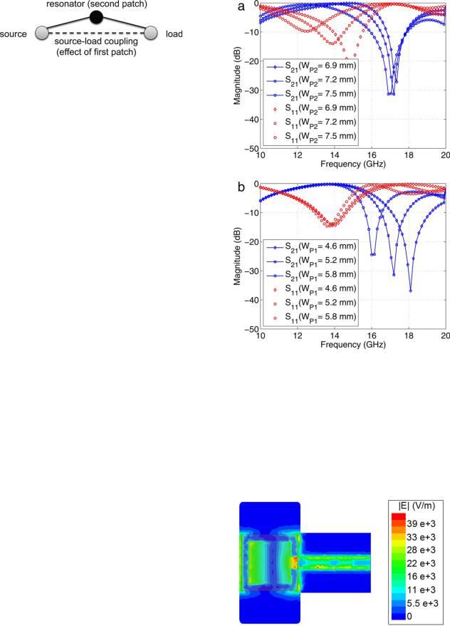
Figure 2 Coupling and routing scheme of the transition with two patch elements
3. DESIGN GUIDELINES AND DISCUSSION
This kind of a transition having a resonator as a matching element is analogous to a single-pole coupled resonator bandpass filter with source-load cross-coupling, as shown in Figure 2. It has been shown that a resonating filter with n resonators could have up to n transmission zeros if the source and the load are cross-coupled [6]. The second patch is the main resonator in this system whose dimension, WP2, determines the passband characteristics as shown in Figure 3(a). The first patch, on the other hand, plays the role of source-load cross-coupling and its dimension, WP1, modifies the out-of-band response. A larger WP1 results in a larger cross-coupling between source and load, resulting in a frequency shift of the transmission zero toward the center frequency [7], as can be seen in Figure 3(b).
The transition design is simulated using Ansys HFSS. Figure 4 shows the electric field distribution on the substrate at 13.8 GHz.
Excitation of the TM01 mode beneath the patch antenna can be clearly observed.
To design this transition, one can estimate the dimensions of the second patch, WP2, using
k0=3 WP2 k0=2 |
(1) |
where k0 is the wavelength at center frequency, f0. Due to the proximity of the patch to the waveguide side walls and the resulting fringing fields, the patch dimensions need to be tuned very close to the lower bound of Eq. (1) to achieve the desired resonant frequency. The dimension WP1 of the first patch determines the magnitude of the cross-coupling coefficient, which specifies the location of the transmission zero. One can achieve a broader frequency bandwidth by moving the frequency of the transmission zero away from the passband. Since no closedform solution exists for this phenomenon, numerical simulation and optimization can be performed to find the optimal dimensions.
Increasing the distance hG between the patch and its ground results in a broader bandwidth at the expense of the increased volume. The channel width of the suspended stripline, WC, must be carefully selected for a proper transmission response. The metallic guide hosting the SSL also serves as a rectangular waveguide of dimensions WC 3 1 mm. In order to prevent any waveguide mode from propagating within this guide, WC needs to be narrower than a half wavelength. Under this condition, only the SSL mode will propagate as all the waveguide modes are evanescent.
4. FABRICATION AND MEASUREMENT
Two WG–SSL transitions were cascaded in a back-to-back configuration to form an SSL–WG–SSL transition. For measurement purposes, two end-launch SMA connectors were also added to the SSL ports. Photographs of this transition are shown in Figures 5(a) and 5(b).
Figure 3 Variation of the simulated frequency responses of the WG– SSL transition with respect to WP1 and WP2. (a) Adjustment of WP2 with WP1 55.2 mm. (b) Adjustment of WP1 with WP2 57.2 mm. [Color figure can be viewed in the online issue, which is available at wileyonlinelibrary.com]
To remove the effect of the SMA connectors and the coax- to-SSL transitions, a standard thru-reflect-line (TRL) calibration was performed and the measurement plane was set at the broad wall of the waveguide (See Figure 1). Figure 5(c) shows a photograph of the TRL calibration kit.
Figure 4 Electric field strength on the substrate at the center frequency 13.8 GHz for an incident power of 1 W. [Color figure can be viewed in the online issue, which is available at wileyonlinelibrary.com]
1832 |
MICROWAVE AND OPTICAL TECHNOLOGY LETTERS / Vol. 58, No. 8, August 2016 |
DOI 10.1002/mop |

Figure 5 Photographs of the fabricated parts. (a) Dismantled SSL– WG–SSL transition. (b) Assembled SSLWG–SSL transition. (c) Dismantled calibration kit standards. [Color figure can be viewed in the online issue, which is available at wileyonlinelibrary.com]
Figure 6 Simulated and measured frequency responses of the SSL– WG–SSL transition. [Color figure can be viewed in the online issue, which is available at wileyonlinelibrary.com]
TABLE 1 Measured Results of Several WG–SSL and WG–MS
Transitions
Paper |
Output |
BW (at RL) |
IL (at f0) |
Back-short |
[2] |
MS |
16% (10 dB) |
0.25 dB (30 GHz) |
kg/4 |
[3] |
MS |
10% (15 dB) |
0.30 dB (76 GHz) |
None |
[4] |
SSL |
5.7% (14 dB) |
0.21 dB (26 GHz) |
kg/10 |
This |
SSL |
12% (10 dB) |
0.09 dB (14 GHz) |
kg/30 |
|
|
|
|
|
Scattering parameters of the back-to-back transition were measured with an Agilent N5230A network analyzer. Figure 6 compares the measured and simulated frequency responses of the SSL–WG–SSL transition. Except for a slight shift in the center frequency, the simulated and measured results show an excellent agreement. The IL of the back-to-back transition is 0.18 dB at 13.8 GHz, making the IL of a single transition equal to 0.09 dB. The 10-dB reflection loss (RL) bandwidth of 12% is observed in measurement.
The resonance around 17 GHz is due to the two transition junctions and the WG transmission line in-between, which together form a resonant structure. The cavity formed by the waveguide and two transitions at both ends will resonate when the length of the waveguide becomes an integer multiple of a half wavelength, which occurs around 17 GHz for the lowestorder mode.
5. COMPARISON
Table 1 compares the transition characteristics of this work with other WG–SSL transitions as well as several WG–MS transitions. This work uses patch elements to reduce the size and lower the IL of the transition for a comparable BW, as opposed to using a simple probe and a long back-short in Ref. 2. The BW of the WG–MS transition in Ref. 3 is comparable to that in this design. It does not need a back-short but it still needs a cover plate to shield the MS from surrounding environment. The WG-SSL in Ref. 4 needs a longer back-short and its measured BW is narrower than this design.
6. CONCLUSION
A compact low-loss, broadband perpendicular WG–SSL transition has been presented. It utilizes patch resonators as a matching device to convert between the TEM mode of an SSL and the TE10 mode of a rectangular waveguide. A back-to-back SSL–WG–SSL transition has been designed in Ku band with a thin, low-loss, high frequency dielectric substrate. Using a proximity feed yielded a 12% frequency bandwidth. A singletransition IL as low as 0.09 dB at 13.8 GHz has been achieved in measurement.
ACKNOWLEDGMENT
This work was supported by the National Oceanic and Atmospheric Administration (contract NRMC0009-12-02700).
REFERENCES
1.Y. Deguchi, K. Sakakibara, N. Kikuma, and H. Hirayama, Millimeterwave microstrip-to-waveguide transition operating over broad frequency bandwidth, In IEEE MTT-S International Microwave Symposium Digest, Long Beach, CA, June 2005, pp. 2107–2110.
2.F.J. Schmuckle, W. Gross, K. Hirche, M. Rostewitz, and W. Heinrich, A 30-GHz waveguide-to-microstrip-transition, In Proceedings of IEEE MTT-S International Microwave Symposium, Honolulu, Hawaii, June 2007, pp. 1169–1172.
DOI 10.1002/mop |
MICROWAVE AND OPTICAL TECHNOLOGY LETTERS / Vol. 58, No. 8, August 2016 |
1833 |

3.W. Grabherr, B. Huder, and W. Menzel, Microstrip to waveguide transition compatible with mm-wave integrated circuits, IEEE Trans Microwave Theory Tech 42 (1994), 1842–1843.
4.R. Glogowski, J.F. Zurcher, C. Peixeiro, and J.R. Mosig, Ka-ban- drectangular waveguide to suspended stripline transition, IEEE Microw Compon Lett 23 (2013), 575–577.
5.M.A. Nikravan and D.-H. Kwon, A vertical waveguide-to-suspended stripline transition, In: Proceedings of IEEE Antennas and Propagation Society International Symposium, Memphis, TN, July 2014, pp. 1696–1697.
6.S. Amari, U. Rosenberg, and J. Bornemann, Adaptive synthesis and design of resonator filters with source/load-multiresonator coupling, IEEE Trans Microwave Theory Tech 50 (2002), 1969–1978.
7.I. Awai, A.C. Kundu, and T. Yamashita, Equivalent-circuit representation and explanation of attenuation poles of a dual-mode dielectricresonator bandpass filter, IEEE Trans Microwave Theory Tech 46 (1998), 2159–2163.
VC 2016 Wiley Periodicals, Inc.
A COMPACT INTERNAL ANTENNA FOR LTE/WWAN MOBILE PHONE APPLICATIONS
Cheng-Chi Yu,1 Jiin-Hwa Yang,2 and Chang-Chih Chen1
1Department of Communications Engineering, Feng-Chia University, , Taichung, Taiwan 40724, R.O.C
2Ph.D. Program in Electrical and Communications Engineering, Feng-Chia University, No.100, Wen-Hua Rd, Seatwen, Taichung, Taiwan 40724, R.O.C; Corresponding author: jyang@nkut.edu.tw
Received 14 December 2015
ABSTRACT: A compact multiband internal antenna is proposed for LTE/ WWAN mobile phone application. The structure of proposed antenna is composed of a coupling feed L-shaped monopole and a grounded meandered branch. The coupling feed L-shaped monopole excites a widely operating band to cover the frequency range of 1750 2525 MHz for the DCS/
PCS/UMTS/LTE/WLAN operation. The grounded meandered branch excites the low frequency operation band to cover the frequency range of
675 985 MHz for the LTE700/GSM operation. The antenna occupies a small volume of 4 3 14 3 45 mm3 only. The measured result of the 6 dB return loss meets for each operating band. Moreover, the antenna gain and efficiency are measured in good performances. The measured radiation patterns are similar to general monopole antenna. The characteristics of the proposed antenna make it attractive for slim mobile phone applications. VC 2016 Wiley Periodicals, Inc. Microwave Opt Technol Lett 58:1834–1838, 2016; View this article online at wileyonlinelibrary.com. DOI 10.1002/mop.29919
Key words: L-shaped monopole; meandered branch; coupling feed; LTE; WWAN
1. INTRODUCTION
In recent years, the industry of mobile communication has been growing rapidly, and the need of its function is getting stronger. An antenna is one of the most important device in wireless communication system. It plays an important role in transmission distance, and signal strength. Therefore, an antenna plays an important role in mobile communication. For mobile phone, it is necessary to design an antenna with multiband coverage of LTE/GSM/UMTS/WLAN.
Nowadays, a mobile phone is required to be light, thin, and small. Within a limited space, it is challenge for an antenna engineer to design these bands in an antenna. Generally, most mobile phone antennas are planar inverted-F antenna (PIFA)
Figure 1 The geometry and dimensions of the proposed antenna. [Color figure can be viewed in the online issue, which is available at wileyonlinelibrary.com]
[1,2], or monopole antennas [3,4]. Those belong to printed microstrip antennas. They are easy to be integrated into RF circuits and have advantages such as easy to be made, low cost, and small volume, which meets the needs mentioned above.
As to the design of dualband antenna, the most common way is to use two branches with different length to reach dual-band [5,6], or to use dual frequency exciting mode so that a path can produce two frequencies [7]. Some multiband antennas are designed by stretching a dualband antenna and adding quarter wavelength branch under a certain frequency [8,9], or digging a slot on ground so that another resonance path is produced [10]. Other design adds a parasitic element on the back of radiator [11] so that current passes through with coupling which can excite another mode.
A meandered structure antenna with multiband operation for smart phones is proposed. In order to reduce the dimension, a solid bend is made on the end of the meandered branch. A coupling feed L-shaped monopole is used in the antenna. The meandered radiator is on the same side of ground plane. The volume of the antenna is only 14 3 45 3 4 mm3 and makes it suitable for the LTE/GSM/UMTS/WLAN operation.
2. THE PROCEDURE OF ANTENNA DESIGN
The geometry and dimensions of the proposed multiband antenna are shown in Figure 1. A 0.8-mm thick FR4 substrate (er 5 4.4, tand 50.022) is used as the system circuit board. The
1834 |
MICROWAVE AND OPTICAL TECHNOLOGY LETTERS / Vol. 58, No. 8, August 2016 |
DOI 10.1002/mop |