

диафрагмированные волноводные фильтры / 32da18e5-27ea-4020-a7ff-910a54b86fd4
.pdfProceedings of the 44th European Microwave Conference
Reconfigurable E-plane Waveguide Resonators For
Filter Applications
N. Mohottige*, B. Bukvic*^, D. Budimir*
*Wireless Communications Research Group, University of Westminster 115 New Cavendish Street, London, W1W 6UW, UK d.budimir@wmin.ac.uk
^School of Electrical Engineering, University of Belgrade, Serbia
Abstract—This paper presents reconfigurable E-plane waveguide resonators at X-band. A graphene based switch and a silicon switch is used as the switching elements and is connected to the edge of a metallic fin. Through electrical biasing of the graphene or optical illumination of the silicon dice, a different length of the fin is realized, thus creating a shift in resonant frequency of the structure. Frequency shift of about 4.5% is achieved for the resonator using the graphene switch. As a reference, measured results of a fabricated optically reconfigurable resonator are compared to that of the simulated results of the graphene based reconfigurable resonator.
Keywords— Inline filters, E-plane filters, reconfigurable filters, extracted pole filters, graphene based switches, waveguide.
I.INTRODUCTION
Waveguide filters offer a sustainable solution for low-cost, low-loss and high power filters for modern microwave and millimeter-wave applications. Current advancements in communication systems have enthused new challenges for development of more compact RF front end modules which nowadays are required to communicate through various frequency bands. Tuneable and reconfigurable filters have a distinct advantage for such modules as they are capable of providing compactness for these multifunctional systems.
Tuneable and reconfigurable waveguide filters have previously been proposed using magnetic tuning such as YIG [1][2], and micro-electromechanical system (MEMS) switches [3][4]. Electronic tuning using varactor diodes [5][6] as well as using ferroelectrics [7] have been proposed for coplanar or micro-strip based devices. Recently an optically reconfigurable E-plane waveguide resonator using silicon based switches was proposed in [8].
The recent discovery of carbon based 2D material, graphene, has opened new opportunities for development of tunable/reconfigurable devices. Examples of such devices include patch antennas [9], antenna phase shifters [10] and filters [11]. However, most of these applications are designed for the THz frequency range and are not suitable for microwave frequencies. Apart from this only a few lower frequency applications has been presented, including graphene based switches [12]. In this paper we introduce our graphene based switch and its application for a reconfigurable E-plane
waveguide resonator in the X-band. The paper is divided in to the following chapters: In chapter II we give present the theoretical model of graphene based switch and its operation. Chapter III gives a brief description of the E-plane waveguide resonator employed. Chapter IV summarises observed results and concludes in chapter V.
II.THE GRAPHENE BASED SWITCH
Graphene is the first discovered 2D material, and can be modelled by its surface conductivity as a tensor in the most general form. Assuming low frequency (roughly below about 500 GHz), zero magnetic fields and no doping with other material, the surface conductivity of graphene, σ, can be presented by the approximated formula [13]:
|
|
|
qe |
|
Kb T |
|
|
μc |
|
|
|
Kb T |
|
|
|
||||||||
|
|
|
|
|
2 |
|
|
|
|
|
|
|
|
|
|
|
|
|
μc |
|
|
|
|
σ = − j |
|
|
|
|
|
|
|
|
|
|
|
|
|
|
|
+ 2 ln(e |
|
+1) |
|
||||
|
|
|
|
|
|
|
|
|
|
|
|
|
|
|
|
|
(1) |
||||||
π |
= |
2 |
|
(ω |
− |
j |
|
2 |
) |
K |
b |
T |
|
||||||||||
|
|
|
|
|
|
|
Γ |
|
|
|
|
−1 , |
|
|
|
||||||||
Where j |
represents |
|
imaginary |
constant |
Kb |
|
denotes |
||||||||||||||||
Boltzmann constant, T is temperature, ω is angular frequency, Γ signifies scattering rate and µc is chemical potential. Scatering rate is defined as Γ = 1/2τ. Surface conductivity thus consists of both real and imaginary parts.
For our applications, due to relatively high scattering rate (τ = 0.025 ps) [14] and low frequency (below 100 GHz), the imaginary part does not significantly contribute to overall conductivity. Varying µc results in a change in the real part of σ. Thus this characteristic behaviour of graphene is utilized in order to realise the switch. The structure of proposed switch is shown in Fig. 1.
Fig. 1. Proposed graphene based switch.
978-2-87487-035-4 ♥ 2014 EuMA |
299 |
6-9 Oct 2014, Rome, Italy |
In order to demostrate reconfigurability of proposed switch, the structure is simulated in CST with different bias voltages. This biasing will affect µc directly and change it in a range from 0 eV to 1 eV. Simulated results are shown in Fig. 2a and in Fig. 2b for µc = 0 eV and µc = 1 eV, respectively. The dimensions of graphene patch are L = 0.5 mm, W = 0.4 mm, thickness of dielectric is H = 0.5 mm, where its dielectric permittivity is 2.2 and M is metallization thickness.
(a)
(b)
Fig. 2. S-parameter responses of the graphene based switch: (a) Switch OFF;
(b) Switch ON.
III.RECONFIGURABLE E-PLANE RESONATORS
In this section we give a comparison of a reconfigurable E-plane waveguide resonators using silicon based switch and the proposed graphene based switch. The resonant structure used here is based on the principle operation of E-plane extracted pole waveguide sections (EPS). The E-plane EPS is formed modifying the conventional E-plane resonator through the addition of a single metallic fin, located between two septa and grounded on one side through the top broad wall of the waveguide housing.
The schematic representation of an EPS is composed of a resonator connected through an inverter with a FIS element, as shown in Fig. 3a. The shunt FIR element is also referred to as a non-resonating node (NRN). In Fig. 3b, an equivalent representation of an EPS is given as a coupling scheme composed of two nodes: resonating and non-resonating. The inverter is presented as a line connecting the nodes.
|
jB |
jB Resonator |
|
sC |
|
|
sC |
|
|
J |
|
jBN |
jBN |
NRN |
|
Fig. 3. Extracted pole section: (a) schematic representation; (b) coupling scheme representation.
A. Optically reconfigurable E-plane waveguide resonator
A single high resistivity silicon dice, measuring the same width as that of the fin is placed at the open end of the fin as shown by the configuration in Fig. 4.
Metallic Fin
Silicon Switch
Drilled hole for Laser diode
Top Wall
Metallic Septa
Waveguide Housing
Fig. 4. Inside view of an optically reconfigurable E-plane extracted pole section.
The resonant frequency of an E-plane EPS can be controlled either through varying the length of the section (distance between two septa), or by changing the length of the fin. Here we will use the second method as it allows direct control of the pole and the zero. The silicon in its dark state will allow the structure to approximately resonate at the same frequency as the conventional EPS. Under illumination by sufficient level of optical power (200mW), the silicon dice changes state from an insulator to a moderate conductor. This in turn creates an electrical connection is formed between the fin and the silicon and results in extending the length of the fin. By controlling the intensity of the light we can control the conductivity of the silicon dice. The silicon used here is n-type doped with phosphorus to increase its static conductivity from 0.439×10⁻³ S/m to 16.67×10⁻³ S/m. The infra red laser diode used here for illumination of the silicon dice has a 980 nm wavelength, with optical power of 200 mW.
B.Reconfigurable E-plane waveguide resonator using graphene switch
The principle of tuning can be explained as follows. The graphene switch in its unbiased state will allow the structure to approximately resonate at the same frequency as the conventional EPS. Through electrical biasing of the grpahene switch, the mono layer graphene changes state from an insulator to a perfect conductor. Thus an electrical connection is formed between the fin and the graphene based switch. This in turn results in extending the length of the fin. Fig. 5 shows the configuration of the EPS utilizing the graphene based switch.
Fig. 5. Inside view of a reconfigurable EPS using graphene switch.
300

IV. DESIGN OF THE RECONFIGURABLE RESONATORS
E-plane waveguide resonators with two switchable frequency states, one at 10.25 GHz and the other at 9.7 GHz has been designed and simulated. The model of the metallic inserts using the graphene based switch is shown in Fig. 8 and the modelled waveguide cavity comprises of the following non idealities.
The cavity used for housing the inserts is a WR-90 (22.86 mm×10.16 mm) waveguide section constructed out of brass or alluminium. The waveguide resonator consists of two metallic septa and a single fin cut out from a piece of copper, which forms the E-plane EPS.
For the optically reconfigurable resonator, A small piece of silicon with dimensions 3.0 mm×1.25 mm and 0.3 mm thickness is connected on to the metallic fin using silver loaded epoxy. The waveguide housing is constructed out of aluminium and a small hole with a diameter of 5.6 mm is drilled on one side to hold a laser diode with TO18 packaging.
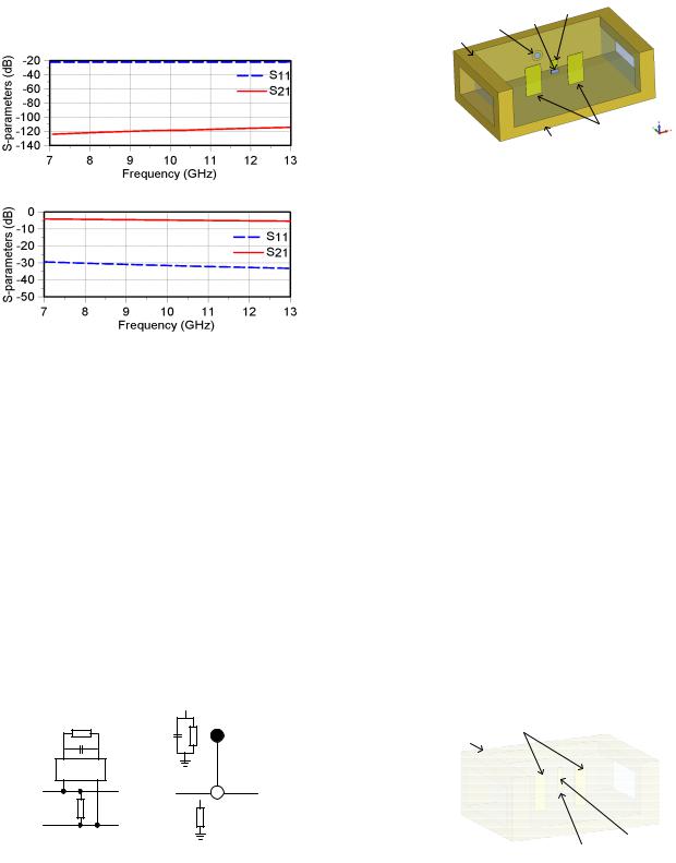
The resonant structure was plotted on copper foil with 0.1mm thickness and placed within the custom build waveguide housing. Measurement results were taken using Anritsu 37397D Vector network analyser. Comparison between the simulated and the measure results are given in Fig. 6 and Fig. 7 [8].
|
0 |
|
|
|
|
(dB) |
-10 |
|
|
|
|
|
|
|
|
|
|
S-Parameters |
-20 |
|
|
|
|
-30 |
|
S11 |
Simulated (OFF) |
||
|
|
||||
|
|
|
|||
|
|
|
S21 |
Simulated (OFF) |
|
|
|
|
S11 |
Measured (OFF) |
|
|
|
|
S21 |
Measured (OFF) |
|
|
-40 |
|
|
|
|
|
9 |
10 |
11 |
12 |
|
Frequency (GHz)
Fig. 6. Simulated and measured S-parameters of the optically reconfigurable resonator in OFF State.
|
0 |
|
|
|
|
|
|
S21 |
Simulated |
|
|
|
S21 |
Measured |
|
-10 |
|
S11 |
Simulated |
(dB) |
|
S11 |
Measured |
|
|
|
|
|
|
S-Parameters |
-20 |
|
|
|
-30 |
|
|
|
|
|
|
|
|
|
|
-40 |
|
|
|
|
9 |
10 |
11 |
12 |
Frequency (GHz)
Fig. 7. Simulated and measured S-parameters of the optically reconfigurable resonator in ON State.
In the case of the reconfigurable resonator using the graphene switch, a mono layer of graphene with dimensions 0.4 mm × 0.6 mm is deposited on a substrate with thickeness of 0.5mm and permittivity of 2.2. The layout of the reconfigurable E-plane metal insert is shown in Fig. 8 below together with its dimensions obtained through optimisation as given in Table 1.
(a)
(b)
Fig. 8. Layout of the proposed resonator: (a) reconfigurable E-plane EPS; (b) fin with graphene based switch.
TABLE I. DIMENSIONS (IN MM) OF THE INSERT FOR RECONFIGURABLE
RESONATOR
Parameters |
Values |
Parameters |
Values |
|
Wsep1 |
1.3 |
Hres |
6.0 |
|
Wsep2 |
1.3 |
HWG |
10.16 |
|
Lres |
8 |
Lgraphene |
0.6 |
|
Wres |
0.4 |
Graphene |
0.4 |
|
Width |
||||
|
|
|
By changing bias voltage, µc will be altered and in turn it will create a change in surface conductivity of graphene. As mentioned before, for the situation where the magnetic field is absent and for frequencies bellow the THz range, only the real part of graphene surface conductivity will be changed. Dimensions of the graphene patch is carefully chosen such that for µc = 0 eV the patch acts like dielectric material, whereas for µc = 1 eV the patch behaves very similar to a good conductor. In this way, effective length of the fin can be changed in the same manner as it was done with optical switch.
Biasing of the graphene based switch could be achieved by a wire placed inside waveguide housing. This wire will be connected to the ground plate of the switch and therefore can alter the potential of ground plate. Because the graphene patch is on similar potential to that of the waveguide housing the switch (consisting of layers ground-dielectric-graphene) will
301

behave similar to a charged capacitor. The electric field inside that capacitor is static and it is perpendicular to the graphene patch, such that the field will polarize the patch. Thus, by changing potential of mentioned wire from outside, we will change surface conductivity of graphene and we will obtain effective change in length of fin which at the end will cause frequency shift of the resonator. The simulated S-parameter responses of the reconfigurable EPS in it’s ‘OFF’ and ‘ON’ states is shown in Fig. 9.
|
0 |
|
|
|
(dB) |
-10 |
|
|
|
|
|
|
|
|
S-Parameters |
-20 |
|
|
|
-30 |
|
|
|
|
|
S11-Uc = 1eV |
|
|
|
|
|
|
|
|
|
|
S21-Uc = 1eV |
|
|
|
|
S11-Uc = 0eV |
|
|
|
-40 |
S21-Uc = 0eV |
|
|
|
|
|
|
|
|
7 |
9 |
11 |
13 |
|
|
Frequency (GHz) |
|
|
Fig. 9. Simulated and measured S-parameters of the optically reconfigurable resonator in ON and OFF States.
The graphene based switch has been modelled in CST using the calculated surface impedance of a monolayer graphene from (1). The simulated shift of the resonant frequency of the EPS between ‘ON’ and ‘OFF’ state is 450 MHz (9.7 GHz-9.25 GHz) which relates to a 4.5% shift in frequency. The simulated insertion loss at ‘OFF’ and ‘ON’ centre frequencies are 1.7 dB and 2.1 dB. It can be observed that the results of the reconfigurable EPS using the graphene based switch show similar performance to that of the optically reconfigurable EPS in ‘ON’ State. A prototype of the resonator will be fabricated in a future date to validate the simulated results.
V.CONCLUSION
A new concept of a reconfigurable switching element using graphene for E-plane waveguide resonators has been proposed. The switch has been modelled as a mono layer of graphene with specific dimensions on substrate with εr = 2.2, and was placed at the end of the metallic fin. Electrical biasing of the switch leads to extension of the metallic fin, thus down shifting the centre frequency of the resonator. A frequency shift of about 4.5% was achieved. Measured results of an optically reconfigurable EPS are used as a reference in order
to validate the design method. A prototype of the filter is to be fabricated in later stage to validate the simulated results.
ACKNOWLEDEGEMENT
Financial support was provided by the EU-Erasmus Mundus Action 2 project EUROWEB.
REFERENCES
[1]J. Uher, W.J.R. Hoefer, "Tunable microwave and millimeter-wave bandpass filters," Microwave Theory and Techniques, IEEE Transactions on
,vol.39, no.4, pp.643-653, Apr 1991
[2]P. Bernardi, F. Valdoni, "Fundamentals of a new class of magnetically tunable waveguide filters," Magnetics, IEEE Transactions on , vol.2, no.3, pp. 264268, Sep 1966.
[3]Sang-June Park, I. Reines, C. Patel, G.M Rebeiz, "High-Q RF-MEMS 4–6-GHz Tunable Evanescent-Mode Cavity Filter," Microwave Theory and Techniques, IEEE Transactions on , vol.58, no.2, pp.381-389, Feb. 2010.
[4]Winter Dong Yan, R.R Mansour, "Tunable Dielectric Resonator Bandpass Filter With Embedded MEMS Tuning Elements," Microwave Theory and Techniques, IEEE Transactions on , vol.55, no.1, pp.154160, Jan. 2007.
[5]L. Athukorala, D. Budimir, "Compact Second-Order Highly Linear Varactor-Tuned Dual-Mode Filters With Constant Bandwidth,"
Microwave Theory and Techniques, IEEE Transactions on , vol.59, no.9, pp.2214-2220, Sept. 2011.
[6]L. Athukorala, D. Budimir, "Open-loop tunable resonators and filters with constant bandwidth," Microwaves, Antennas & Propagation, IET , vol.6, no.7, pp.800-806, May 16 2012.
[7]S. Courreges, Li Yuan Li, Zhao Zhiyong, Choi Kwang, A. Hunt, J. Papapolymerou, "Ferroelectric Tunable Bandpass Filters for Ka-Band Applications," Microwave Conference, 2008. EuMC 2008. 38th European , vol., no., pp.55-58, 27-31 Oct. 2008.
[8]N. Mohottige, D. Budimir, C. J. Panagamuwa, "Optically reconfigurable E-plane waveguide resonators and filters," Microwave Conference (EuMC), 2013 European , vol., no., pp.798,801, 6-10 Oct. 2013.
[9]M. Tamagnone, J. S. Gomez-Diaz, J. R. Mosig, and J. PerruisseauCarrier, “Reconfigurable THz Plasmonic Antenna Concept Using a Graphene Stack,” Appl. Phys. Lett. 101,214102, 2012.
[10]Pai-Yen Chen; Argyropoulos, C.; Alu, A., “Terahertz Antenna Phase Shifters Using Integrally-Gated Graphene Transmission-Lines, ” Antennas and Propagation, IEEE Transactions on , vol.61, no.4, pp.1528,1537, April 2013.
[11]D. Correas Serrano, J. S. Gomez Diaz, J. Perruisseau-Carrier, and A. Alvarez Melcon, “Graphene Based Plasmonic Tunable Low Pass Filters in the THz Band,”, arXiv:1304.6320v1 [cond-mat.mes-hall], 2013.
[12]J. S. Gomez-Diaz, and J. Perrusseau-Carier, “Graphene-based plasmonic switches at near infrared frequencies”,Optics Express, vol. 21, issue 13, pp. 15490-15504, 2013.
[13]Hanson, G. W., “Dyadic Green's Functions for an Anisotropic, NonLocal Model of Biased Graphene,” Antennas and Propagation, IEEE Transactions on , vol. 56, no. 3, pp.747,757, March 2008
[14]J. S. Gomez-Diaz, J. Perruisseau-Carrier, P. Sharma, and A. Ionescu,
“Non-contact characterization of graphene surface impedance at micro and millimeter waves,”Journal of Applied Physics,vol. 111, no. 11, pp. 114908, 114908-7, Jun 2012.
302