

диафрагмированные волноводные фильтры / 03e9c394-e281-45a0-8b2d-0175daa4edc7
.pdf2005 Asia-Pacific Conference on Communications, Perth, Western Australia, 3 - 5 October 2005.
Design of the Multipaction Free High Power Ka-band Diplexer with an E-plane T-junction
So Hyeun Yun, Man Seok Uhm, In Bok Yom
Communication Satellite RF Technology Team
Electronics and Telecommunications Research Institute (ETRI) 161 Gajeong-dong, Yuseong-Ku, Daejeon, 305-700, Korea
Tel.: +82-42-860-4920, FAX.: +82-42-860-6949, E-mail: yoonsh@etri.re.kr
Abstract-In this paper, the design and performance of a low-PIM and multipaction free Ka-band (20/30GHz) waveguide diplexer with an E-plane T-junction is described. The waveguide diplexer consists of a transmit filter and a receive filter combined to the antenna port via an E-plane T-junction. The reason why E-plane T-junction structure was selected is to reduce PIM (Passive Intermodulation) level. In order to handle high power the multipaction analysis was performed in design stage as the peak voltage in the resonator with minimum gap is much smaller than the threshold voltage recommended by ESA/ESTEC. The multipaction analysis margin is greater than 12dB. The manufactured diplexer has good pass band return loss (>24dB) and high isolation (>52dB) for both transmit and receive frequency bands. The diplexer does not need any post fabrication tuning. Those mean the analysis results of the waveguide diplexer are verified through the electrical performance test.
I. INTRODUCTION
A diplexer is a device for either splitting a frequency range band into sub-bands or combing two sub-bands into one wide frequency band. A diplexer is widely used for the satellite communication system because the use of combined transmit/receive antennas on spacecraft can reduce the mass and volume by a considerable amount [1]. Antenna diplexers for satellite communication systems are subject to severe electrical and mechanical constraints. Among the more important electrical constrains, the low insertion losses, the very low level of PIM (Passive Inter-modulation) and the sufficient multipaction margins are required. An accurate computer aided design is necessary to avoid the need for tuning screws or any additional adjustments, which limit the maximum transmittable power, generate PIM products, and increase the cost of the device [2].
A diplexer consists of a transmit filter, a receive filter and a manifold to combine two filters. This arrangement allows the high power transmit carriers to generate intermodulation products in the receive band. These products can be a similar power level to the receive signals and can therefore pose a severe problem in systems design. PIM products are generated in the waveguide diplexer by bad metal to metal contacts, dissimilar metal contacts, microcracks and so forth
[3]. In order to reduce PIM levels, it is appropriate for a device to be silver-plated and manufactured by splitting the broad wall of the filters and manifold to ensure very low electrical current across the interface. It is for this reason that an E-plane T-junction, not an H-plane, is chosen for manifold.
E-field analysis of cavity resonators in filters shows that voltage enhancement takes place in the resonators due to cavity resonance in high Q cavities. Multipaction is a RF breakdown phenomenon, which takes place in the presence of high RF power under vacuum condition in the presence of free electrons. Therefore, it is necessary to perform multipaction risk analysis based on electromagnetic theory at the design phase. Multipaction margin with respect to the operating power is analyzed by comparing the susceptibility zone chart of ESA [4] with the calculated E-field in the resonators [5].
This paper deals with the Ka-band (20/30GHz) waveguide diplexer with an E-plane T-junction as shown in Figure 1. The diplexer was designed optimally and manufactured from aluminum in two halves along the broad wall of rectangular waveguide. It was found from measurement that the RF performances of diplexer without any tuning screws met the specification and the design method was adequate.
Common
Port
TX Port
RX Port
Figure 1 Configuration of the E-plane T-junction Waveguide Diplexer
0-7803-9132-2/05/$20.00 ©2005 IEEE. |
582 |

IIDESIGN OF DIPLEXER
A.Electrical Design
The design begins with the generation of a suitable prototype filter. Corrugated waveguide structures are used as low pass filters in numerous antennas feed system. They are adopted for reducing spurious harmonics from transmitters [6]. The low pass filter for transmit frequency band was designed from stepped distributed proto-type elements to avoid the unwanted spurious mode at the receive frequency band. The initial elements of the stepped distributed low pass proto-type are presented in Table 1 [7].
TABLE 1 ELEMENT OF THE STEPPED-DISTRIBUTED LOW PASS PROTOTYPE
Z1 |
Z9 |
1.213 |
Z2 |
Z8 |
0.6972 |
|
|
|
|
|
|
Z3 |
Z7 |
1.790 |
Z4 |
Z6 |
0.5359 |
|
|
|
|
|
|
Z5 |
|
2.011 |
|
|
|
The receiving filter was designed for TE101 mode directcoupled cavities and inductive iris used commonly in waveguide filter, especially at higher frequency, due to low loss and high temperature stability. The filter was designed to be of 3-pole due to low insertion loss and band rejection in the transmit frequency range.
Two filters and a T-junction that were optimally designed in advance were plugged in to the diplexer. Even if filters and a T-junction each were designed well, the RF performance of whole diplexer hardly ever achieves the wanted value, simultaneously in both pass bands. This is mainly due to the variation of the phase of reflection coefficient from filters and the higher order mode in the pass bands. Therefore, the whole diplexer needs to be effectively re-optimized by the sequential method as follows.
The optimization was performed on the equivalent circuit shown in Figure 2. The E-plane waveguide steps of corrugated low pass filter and inductive irises of band pass filter were modeled based on the equations given in Marcuvitz [8]. Initially, only manifold and branch guide
lengths (LRx and LTx) formerly determined [1] by replacing each filters with short circuit were optimized. Gradually more components were added to the optimization until the resonances and couplings from each were modified to recover the return loss response on the manifold. Next, the transmission line elements were realized as physical waveguide dimensions by using 3D FEM field simulator. The analysis of a symmetric and thick iris in rectangular waveguide and an E-plane waveguide step yield complex scattering matrix elements. Finally, the physical dimensions of whole diplexer were checked by 3D FEM field simulator. The predicted performance of the optimized diplexer is presented in Figure 3. The return loss and the isolation are greater than 23dB and 50dB for both transmit and receive bands, respectively.
|
0 |
|
|
|
|
|
|
|
|
|
|
|
|
|
|
|
-10 |
|
|
|
|
|
|
|
|
|
|
|
|
|
|
|
-20 |
|
|
|
|
|
|
|
|
|
|
|
|
|
|
(dB) |
-30 |
|
|
|
|
|
|
|
|
|
|
|
|
|
|
|
|
|
|
|
|
|
|
|
|
|
|
|
|
|
|
Amplitude |
-40 |
|
|
|
|
|
|
Return |
|
|
|
|
|
|
|
|
|
|
|
|
|
|
|
|
|
|
|
|
|||
-50 |
|
|
|
|
|
|
Isolation |
|
|
|
|
|
|||
|
|
|
|
|
|
|
|
|
|
|
|
|
|
||
|
|
|
|
|
|
|
|
|
|
|
|
|
|
|
|
|
-60 |
|
|
|
|
|
|
|
|
|
|
|
|
|
|
|
-70 |
|
|
|
|
|
|
|
|
|
|
|
|
|
|
|
-8018 |
19 |
20 |
21 |
22 |
23 |
24 |
25 |
26 |
27 |
28 |
29 |
30 |
31 |
32 |
Frequency (GHz)
Figure 3 Predicted Performance of the Optimized Diplexer
B. High Power Handling Capability
In order to predict high power handling capability the analysis for PIM and multipaction should be performed. PIM is RF distortion that occurs whenever signals at two or more frequencies conduct simultaneously in a passive device. The nonlinear behavior generates unwanted products whose frequencies are linear combinations of the original signals. The lower odd ordered IM products (e.g. fp=(n-1)(f2-f1)/2+ f2)
|
Inductive iris Band Pass Filter |
|
W/G TE10mode |
|
RX Port |
LRx |
Inductive iris |
Common |
|
port |
TX Port |
|
LTx |
S-parameter |
|
|
|
|
|
|
|
|
|
W/G TE10mode |
|
|
|
|
|
|
|
|
|
||
|
|
|
|
|
|
|
|
|
|
|
(E-plane T- |
|
|
|
|
|
|
|
|
|
|
|
|
|
|
|
|
|
|
|
|
|
junction) |
E-plane W/G step |
|||||||||
Corrugated Low Pass Filter
Figure 2 Equivalent Circuit of the Diplexer
583

are usually the most problematic since they have the highest potential of falling within the receive. The physics lying behind the PIM problem is not well-understood yet. Some known sources of PIM are poor metal contacts, hysteresis of ferromagnetic material, microcracks at metal surface, etc. Normally, the reason for PIM generation at waveguide contacts is the poor metal contact in combination with native oxidation of the waveguide metals and the lack of precision in the fabrication process [9].
Therefore, the diplexer should be manufactured from proper material with the minimum number of contact junctions and no tuning screws. Besides, any possible source of IM generation should be located in regions of low current density to reduce the level of PIM. The diplexer of this paper was machined in two halves from aluminum alloy, and then silver plated. The split in the diplexer was along the broad wall of the filters and manifold to ensure very low electrical current across the interface. The diplexer had no any tuning screw. Due to these reason and very high PIM order, 49th, the low PIM level of the diplexer is predicted.
Multipaction is an electron phenomenon which occurs at radio frequencies in components and transmission lines operating in a vacuum. Multipaction represents a strong possible system failure mechanism since it can destroy RF components or transmission lines, or it can significantly increase system noise floors. Multipaction is a discharge produced in vacuum when an RF field exits between two surfaces. It results from an ion moving back and forth and knocking other electrons off the sides when it strides. As the number of electrons bounding back and forth increases exponentially, the current can increase to a point where a hot spot forms on the cavity walls, increasing outgassing, melting the walls, evaporating material, and all undesirable things. The secondary electron emission (SEE) actually goes down as the electron energy rises over the peak, so breakdown can sometimes be avoided by rapidly raising the incident RF power. If the pressure is high, then the electron will likely hit another gas molecule or atom before hitting the other side, so multipaction is less likely. Therefore the mean free path must be on the order of the spacing for multipaction to occur. Aluminum has a very high SEE coefficient primarily due to oxidation, thus a good idea to plate with silver or gold in waveguide intended for use in vacuum or space applications.
Based on the theory, multipaction susceptibility zones for the different materials were constructed from the experimental data by ESA/ESTEC [4]. The zone boundaries define the actual multipaction threshold expected, without any margin, except for that of the original measurements made.
In TE10 mode, maximum E field occurs at the center of broad wall of rectangular waveguide. Maximum E field also appears at the smallest gap of resonators in the longitudinal direction. The magnitude of E field at the center of silver plated diplexer along the longitudinal direction was calculated as shown in Figure 4. The smallest gap of resonators was 2.32mm, which was the critical region with respect to
multipaction breakdown. The peak voltage in the resonator of 2.32mm gap was calculated by 3D-FEM analysis tool and the results are summarized in Table 2. The threshold gap voltage was obtained from susceptibility zone chart [4]. In the multicarrier case, the recommended multipaction margins are more than 6dB. The calculated maximum handling power of the diplexer is 4.4kW or 12dB multipaction margin above input peak power and is sufficient to satisfy ESA/ESTEC recommendation.
|
18000 |
|
|
|
|
|
|
|
|
|
|
E (V/m) |
15000 |
|
|
|
|
|
|
|
|
|
|
12000 |
|
|
|
|
|
|
|
|
|
|
|
Mag_ |
|
|
|
|
|
|
|
|
|
|
|
Complex |
9000 |
|
|
|
|
|
|
|
|
|
|
|
|
|
|
|
|
|
|
|
|
|
|
|
6000 |
|
|
|
|
f=19.8GHz |
|
|
|
|
|
|
|
|
|
|
|
|
|
|
|
||
|
|
|
|
|
|
f=20.0GHz |
|
|
|
|
|
|
|
|
|
|
|
f=20.2GHz |
|
|
|
|
|
|
30000 |
0.1 |
0.2 |
0.3 |
0.4 |
0.5 |
0.6 |
0.7 |
0.8 |
0.9 |
1 |
Normalized Distance
Figure 4 Magnitude of Complex E-field across center line
TABLE 2 COMPUTED MULTIPACTION MARGINS
Freq. |
Threshold |
Gap Vol. |
Available |
Margin |
(GHz) |
Vol. (V) |
(V) |
Power (W) |
(dB) |
|
|
|
|
|
19.8 |
2866 |
42.97 |
4449 |
12.27 |
20.0 |
2895 |
42.87 |
4560 |
12.37 |
20.2 |
2924 |
43.01 |
4622 |
12.43 |
III EXPERIMENTAL RESULTS
The diplexer was manufactured from aluminum ally in two halves, as shown in Figure 5. The low level of PIM can be expected because the split was along the broad wall of the diplexer and no tuning screws were required. Each part was silver plated for minimum insertion loss, high multipaction margin and preventing corrosion. Two parts were bolted together.
(a) One-half |
(b) Assembled |
Figure 5 Manufactured Waveguide Diplexer
584
|
0 |
|
|
|
|
|
|
|
|
|
|
|
-5 |
|
|
|
|
|
|
|
|
|
|
|
-10 |
|
|
|
|
|
|
|
|
|
|
(dB) |
-15 |
|
|
|
|
|
|
|
|
|
|
-20 |
|
|
|
|
|
|
|
|
|
|
|
Amplitude |
-25 |
|
|
|
|
|
|
|
|
|
|
-30 |
|
|
|
|
|
|
|
|
|
|
|
-35 |
|
|
|
|
|
|
|
|
|
|
|
|
|
|
|
|
|
|
|
|
|
|
|
|
-40 |
|
|
|
|
|
|
|
|
meas |
|
|
|
|
|
|
|
|
|
|
|
|
|
|
-45 |
|
|
|
|
|
|
|
|
comp |
|
|
|
|
|
|
|
|
|
|
spec |
|
|
|
|
|
|
|
|
|
|
|
|
|
|
|
-5019 |
19.2 |
19.4 |
19.6 |
19.8 |
20 |
20.2 |
20.4 |
20.6 |
20.8 |
21 |
|
|
|
|
|
Frequency (GHz) |
|
|
|
|
||
(a) Return Loss for Transmit Frequency Band
|
0 |
|
|
|
|
|
|
|
|
|
|
|
-5 |
|
|
|
|
|
|
|
|
|
|
|
-10 |
|
|
|
|
|
|
|
|
|
|
(dB) |
-15 |
|
|
|
|
|
|
|
|
|
|
-20 |
|
|
|
|
|
|
|
|
|
|
|
Amplitude |
-25 |
|
|
|
|
|
|
|
|
|
|
-30 |
|
|
|
|
|
|
|
|
|
|
|
-35 |
|
|
|
|
|
|
|
|
|
|
|
|
|
|
|
|
|
|
|
|
|
|
|
|
-40 |
|
|
|
|
|
|
|
|
meas |
|
|
|
|
|
|
|
|
|
|
|
|
|
|
-45 |
|
|
|
|
|
|
|
|
comp |
|
|
|
|
|
|
|
|
|
|
spec |
|
|
|
|
|
|
|
|
|
|
|
|
|
|
|
-5029 |
29.2 |
29.4 |
29.6 |
29.8 |
30 |
30.2 |
30.4 |
30.6 |
30.8 |
31 |
|
|
|
|
|
Frequency (GHz) |
|
|
|
|
||
(b) Return Loss for Receive Frequency Band Figure 6 Measured Return Loss
TABLE 3 MEASUREMENT OF THE DIPLEXER
Parameters |
|
Required |
Measured |
|
Operational Freq. (GHz) |
TX |
19.8 – 20.2 |
19.8 – 20.2 |
|
RX |
29.6 - 30.0 |
29.6 - 30.0 |
||
|
||||
Return Loss (dB) |
TX |
> 22 |
> 24.43 |
|
RX |
> 22 |
> 25.43 |
||
|
||||
Insertion Loss (dB) |
TX |
< 0.20 |
< 0.10 |
|
RX |
< 0.20 |
< 0.14 |
||
|
||||
Isolation (dB) |
TX |
> 40 |
> 65.47 |
|
RX |
> 40 |
> 51.61 |
||
|
||||
Group Delay Variation |
TX |
< 0.2 |
< 0.08 |
|
(nsp-p) |
RX |
< 0.2 |
< 0.06 |
|
Multipaction Margin (dB) |
TX |
> 6 |
> 12.3 |
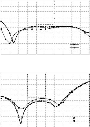
Figure 6 depicts the predicted and experimental return loss, comparing with specification, at both frequency bands for the whole diplexer, obtained with the final optimized dimensions. Excellent agreement can be observed at the low frequency band with a response better than 24dB. A good agreement also observed in high frequency band with return loss better than 25dB. The other computed and measured parameters also
have a good agreement. All of the RF performance parameters are complaint with specifications as presented in Table 3.
IV CONCLUSIONS
In this paper, the Ka-band waveguide diplexer with an E- plane T-junction has been optimally designed and the design method has been verified through the measured results. The diplexer was optimized by using equivalent circuit and the computation time was reduced. The final realization as physical waveguide dimensions was accomplished by 3D FEM field analysis tool. The diplexer, especially the smallest gap of the transmit filter, was also designed to have an enough multipaction margin that is greater than ESA/ESTEC recommendation for high power handling. The diplexer was carefully fabricated to keep the rule of low level of PIM. In a practical manner, not only was the diplexer machined from aluminum in two halves along E-plane and plated them with silver, it also had no tuning screws. The measured results met the specification without any post fabrication tuning.
It is expected that the provided design method of the E- plane T-junction diplexer is efficient for optimization and the implemented diplexer is compatible with the high power system of Ka band.
REFERENCES
[1]M.S. Uhm, J. Lee, D. Bae, I.B. Yom and S.P. Lee, “Ka band Waveguide Diplexer using E-plane T-junction with inductive iris,” APMC-2002, vol. 1, pp. 508-511, 2002.
[2]J. Esteban and J.M. Rebollar, “Design and optimization of a compact Kaband antenna diplexer,” IEEE Antennas and Propagation Society International Symposium, AP-S Digest, Vol. 1, pp. 148-151, 1995.
[3]Connor, G.G., “Elimination of fine tuning in high power, low-PIM diplexers for combined transmit/receive antennas,” Microwave Filters and Multiplexers, IEE Colloquium, pp. 4/1-4/6, 1990.
[4]Spacing Engineering; Multipaction Design and Test, ESA Publications Division, pp. 19-28, 2003.
[5]K.S. Parikh, D.K. Singh, A. Praveen kumar, Ms. Shilpi Rusia, Mrs. K. Sangeetha, “MULTI-CARRIER MULTIPACTOR ANALYSIS OF HIGH POWER ANTENNA TX-TX DIPLEXER FOR SATCOM APPLICATIONS,” 4th International Workshop on Multipactor, Corona, and Passive Intermodulation in Space RF Hardware, ESTEC, Sep., 2003.
[6]J. Uher, J. Bornemann and U. Resenberg, Waveguide Components for Antenna Feed System: Theory and CAD, Artech House Inc. Boston, pp. 200-205, 1993.
[7]R. Levy, “Tables of Element Values for the Distributed Low-pass Prototype Filter,” IEEE Trans. On Microwave Theory and Tech. vol. 13, pp. 514-536, Sep., 1965.
[8]N. Marcovitz, Waveguide Handbook, New York Dover Publications, Inc., 1951.
[9]D. Wolk, J. Damaschke, C. Vicente, B. Mottet, H.L. Hartnagel, “Surface Treatment and Coating for the Reduction of Multipactor and Passive Intermodulation (PIM) Effects in RF Components,” 4th International Workshop on Multipactor, Corona, and Passive Intermodulation in Space RF Hardware, ESTEC, Sep., 2003.
585