

диафрагмированные волноводные фильтры / c14ba469-44f3-4194-9926-a1ae8bf94e1b
.pdfIEEE TRANSACTIONS ON MICROWAVE THEORY AND TECHNIQUES, VOL. 46, NO. 8, AUGUST 1998 |
1085 |
Analysis of Dielectric E-Plane Waveguides
and Design of Filters
Hiroshi Kubo, Member, IEEE, Hiroshi Yamashita, Associate Member, IEEE, and Ikuo Awai, Member, IEEE
AbstractÐ A small-size waveguide made of high-permittivity |
|
|||
ceramic is analyzed. The propagation constants are calculated |
|
|||
approximately by an approach where the electromagnetic fields |
|
|||
outside the waveguide are fully taken into consideration. The |
|
|||
analysis values agree well with the experimental values. The |
|
|||
constants of |
equivalent |
circuit for the metallic strip section |
|
|
are obtained |
by using |
a separate model for the analysis of |
(a) |
|
the structure. Based on these results, bandpass filters (BPF's) |
||||
|
||||
are designed and fabricated. The fabricated BPF's have better |
|
|||
transmission and reflection characteristics than those designed |
|
|||
on the basis of a trough-guide model. |
|
|||
Index TermsÐ Dielectric waveguide, electromagnetic analysis, |
|
|||
filters, waveguide filters. |
|
|
||
|
|
|
(b) |
|
|
I. |
INTRODUCTION |
Fig. 1. (a) Basic structure of DEW. (b) Structure of a DEW BPF. |
|
|
|
|
||
RECENTLY, there has been much interest in the miniaturization of microwave passive components because of the need for a small and lightweight handset for mobile
communications [1]. Dielectric ceramic of high permittivity has the effect of wavelength shortening. Small-size bandpass filters (BPF's) for lower microwave frequency bands based on dielectric waveguide [2] have been developed in this way.
The present waveguide structure is a half-cut of a rectangular metal waveguide filled with high-permittivity ceramic [3], which will be referred to as a dielectric  -plane waveguide (DEW). The high permittivity ceramic (relative permittivity


 ) makes the component size small. The open surface created is convenient for attaching some metallic strip patterns, resulting in a quasi-finline structure.
Analysis data for the propagation characteristics is necessary to design the resonator sections and the coupling sections of DEW filters. Approximate approaches may be effectively applied to the analysis because the field energy is confined in the waveguide and the energy leaking out of the open surface is small due to the high permittivity. The modified waveguide structure with assumed electric walls on the top and bottom surfaces has been analyzed and BPF's have been designed [4]. The center frequency of the fabricated filters agreed with the designed values, but the bandwidth did not give good agreement and the return loss was poor.
In this paper, we analyze a DEW in full consideration of the field expanding outside the open surface. The propagation constants obtained are compared with the experimental values. Then, on the basis of the propagation constants and the analysis
Manuscript received April 24, 1997; revised May 11, 1998.
The authors are with the Department of Electrical and Electronic Engineering, Yamaguchi University, Tokiwadai, Ube-shi 755, Japan.
Publisher Item Identifier S 0018-9480(98)05512-4.
results of the coupling coefficients in the modified structure, several BPF's are designed and fabricated.
II. ANALYSIS
Fig. 1(a) shows the basic structure of a DEW. The waveguide is made of high-permittivity ceramics and the side faces (except one) are coated with metal. Although one side face is exposed to the outer region, the high-permittivity ceramic effectively confines the electromagnetic fields in the waveguide. By forming some metallic strip patterns on the open surface, the waveguide is divided into several resonator sections between cutoff sections. The coupling between two adjacent resonators can be adjusted by the width of the strip. Thus, we can make a multistage filter with a tandem connection of waveguide resonators. Fig. 1(b) shows a twostage DEW filter. 


 and
and 


 denote the width of strips and the length of resonator sections, respectively.
A. Phase Constant
We analyze the propagation characteristics of a basic DEW. For simplifying the analysis, we assume two hypothetical electric walls. Fig. 2 shows the cross section of a DEW with the assumed two electric walls on the planes 


 and
and 


 . It is expected that the presence of these walls do not have much influence on the result because the greater part of field energy is confined in the waveguide with high permittivity.
  denotes the ceramic region of the waveguide and
  denotes the exterior air region

 . The guided waves are assumed to vary in the form of


 , where
  is a real phase constant in the
  -direction. The field of the
0018±9480/98$10.00 ã 1998 IEEE

1086 |
IEEE TRANSACTIONS ON MICROWAVE THEORY AND TECHNIQUES, VOL. 46, NO. 8, AUGUST 1998 |
Fig. 2. Cross section of a DEW with two assumed electric walls on the planes x b; y = a and x 0; y = a.
dominant mode is 

 -like in
  and the electric-field lines expand in the
 -directions in
  . We formulate the fields on the following two assumptions:
  , which is not zero in
  , is approximated as

 in
in  , taking account of the continuity of electric-flux density component normal to the open surface and the high permittivity of
  and
and 

 in both
  and
and  . This is a fairly good approximation in
  and may be a rough approximation in
  . Thus, in
  , the electric field has only an
  -component and the electromagnetic field has no dependence on
  .
.
First, the impedance  on the open surface looking inward is deduced as follows:
We represent the fields in  by the
  -component
 of a magnetic vector potential.
 is given by
(7)
(8)
where 

 denotes the wavenumber in the
  -direction. Using the Fourier transform of
 with respect to
  , we obtain
(9)
(10)
where a bar over a symbol denotes a Fourier transform. Considering 


 on the open surface


 ,
, 

 at
at 

 is obtained as follows:
(11)
Using (10) and (11), the complex power flow  into
into
|
|
|
|
|
|
(1) |
out of the open surface is given by |
|
|
|||||||||||||||
|
|
|
|
|
|
|
|
|
|
|||||||||||||||
where |
|
|
|
|
|
|
|
|
|
|
|
|
|
|
|
|
|
|
|
|||||
|
|
|
|
|
|
(2) |
|
|
|
|
|
|
|
|
|
|
|
|
|
|
|
|
|
|
|
|
|
|
|
|
|
|
|
|
|
|
|
|
|
|
|
|
|
|
|
|
|
||
|
|
|
|
|
|
|
|
|
|
|
|
|
|
|
|
|
|
|
|
|
|
|
|
|
|
|
|
|
|
|
|
|
|
|
|
|
|
|
|
|
|
|
|
|
|
|
|
|
|
|
|
|
|
|
|
|
|
|
|
|
|
|
|
|
|
|
|
|
|
|
|
|
|
|
|
|
|
|
|
|
(3) |
|
|
|
|
|
|
|
|
|
|
|
|
|
|
|
|
|
|
is the wave impedance in the |
-direction in , is a |
|
|
|
|
|
|
|
|
|
|
|
|
|
|
|
|
(12) |
||||||
|
|
|
|
|
|
|
|
|
|
|
|
|
|
|
|
|||||||||
|
|
|
|
|
|
|
|
|
|
|
|
|
|
|
|
|
||||||||
permeability that is common in two regions, is the relative |
|
On the open surface, the relation |
applies. Substitu- |
|||||||||||||||||||||
permittivity in , and is the wavenumber in free space. |
|
|||||||||||||||||||||||
Secondly, we derive the impedance |
|
on the open surface |
tion of (6) and (12) into the relation and some transformations |
|||||||||||||||||||||
looking outward. The fields in can be represented by |
give |
|
|
|||||||||||||||||||||
|
|
|
|
|
|
|
|
|
|
|
|
|
|
|
|
|
|
|
|
|
|
|
|
|
|
|
|
|
|
|
|
|
|
|
|
|
|
|
|
|
|
|
|
|
|
|
|
|
|
(4)
(13)
where
|
|
(5) |
||||
where |
and |
are the amplitude and reflection coefficient |
||||
of |
at |
, respectively. Using (4) and (5), the complex |
||||
power flow |
into the open surface out of per unit length |
|||||
to the |
-direction is given by |
|||||
|
|
|
|
|
|
(6) |
|
|
|
|
|||
where the asterisk means the complex conjugate of the indicated symbol.
|
|
|
|
|
|
|
|
|
|
(14) |
|
|
The left-hand side of (13) represents |
. Since the guided |
|||||||||
mode field satisfies the relation |
, we obtain |
||||||||||
|
|
|
|
|
|
|
|
|
|
|
|
|
|
|
|
|
|
|
|
|
|
|
|
|
|
|
|
|
|
|
|
|
|
|
|
|
|
|
|
|
|
|
|
|
|
|
|
|
|
|
|
|
|
|
|
|
|
|
|
(15)

KUBO et al.: ANALYSIS OF DEW'S AND DESIGN OF FILTERS |
1087 |
Fig. 5. Equivalent T network of the strip section.
Fig. 3. Calculated (Ð) and experimental ( ) dispersion relations of the waveguide with a = 5 mm, b = 3 mm, and "c = 83.
(a) |
(b) |
Fig. 6. Calculated values of normalized series reactance xs, shunt reactance xp, and coupling coefficient k of strip section in Fig. 4(b) with a = 5 mm, b = 3mm, d = 50 mm, and "c = 83 for f = 2:5 GHz.
(c)
Fig. 4. Schematic structure of strip section. (a) Strip section of DEW. (b) Strip section of DEW with two electric walls placed on x = 0 and b planes and one electric wall on y = a + d plane. (c) Cross-sectional view of (b).
The dispersion relations can be obtained by numerically solving (15).
Fig. 3 shows the dispersion relation of the waveguide with 

 mm,
mm, 

 mm, and


 . The analysis results of (15) are plotted by the solid line. The experimental results are plotted as the three small circles. The experimental values were obtained by measuring the resonant frequencies of the DEW with large copper sheets pasted on both end faces with respect to the
  -direction. The analysis results agree well with the experimental values.
B. Coupling Coefficient
The coupling coefficients between resonator sections are required to design filters. The metallic strip sections in Fig. 4(a) having a three-dimensional structure can be precisely analyzed only by using a large-scale computer. We substitute the coupling coefficients of the strip section in Fig. 4(b) for those in Fig. 4(a). In Fig. 4(b), we assume two electric walls placed on 

 and
and  planes and one electric wall on


 plane sufficiently apart from the open surface.
If we choose terminal reference planes at 

 and
and  , the equivalent circuit for the strip section is represented by the T network in Fig. 5 and
 and
and 
 are given by [5]
where |
and |
denote the input impedance to the strip |
|||
section with an electric and a magnetic wall at the |
|
||||
plane, respectively. Let a dominant mode ( |
-like) |
||||
be incident on the |
strip section from |
the -direction. |
|||
|
for the incident wave are calculated at first. We |
||||
consider three regions |
, |
|
inside |
||
the dielectric) and |
|
|
outside the dielectric), |
||
shown |
in Fig. 4(c). The |
fields |
in |
these |
|
regions are represented in (17)±(24), shown at the bottom of
the following page, and |
|
is the reflection coefficient for the |
||
dominant mode |
at |
, and |
, |
, and |
satisfy the relations
(25)
(26)
where
|
positive real, |
||||
|
positive real or negative imaginary |
||||
is given by |
through the relation |
||||
|
|
|
|
|
(27) |
|
|
|
|||
Matching these fields at the boundary 

 in the mean square sense [6], [7], the unknown expansion coefficients
  can be determined. Substituting these fields into the relation at the boundary [8]
(28)
(16)we obtain the normalized impedance of (29), shown at the bottom of the following page.

1088 |
IEEE TRANSACTIONS ON MICROWAVE THEORY AND TECHNIQUES, VOL. 46, NO. 8, AUGUST 1998 |
Using these equations, we calculate 
 and
and 
 for the strip section in DEW with


 mm
mm 

 mm
mm
for a frequency 


 GHz. After confirming the convergency of the numerical solutions, the position of an electric wall
  is chosen as


 mm and the truncation number
  is chosen as


 . In Fig. 6, the calculated values for the normalized series reactance
 and the normalized shunt reactance
  are plotted by the solid lines.
III. DESIGN AND FABRICATION OF BPF
We use the design method for n-stage BPF's according to the following relations [9], [10]:
(30)
(31)
(32)
(33)
(34)
(35)
where 
 and
and 

 are the normalized series and shunt reactances of the
  th strip, respectively,


 is the coupling coefficient between both resonator sections adjacent to the
  th strip,
 is the length of the
  th resonator section,
 is the bandwidth of a BPF,
  is the center frequency,
  is the phase constant calculated in the preceding section, and
 is the normalized element value of a prototype low-pass filter (LPF). Substituting the values of
  and
and 
 of Fig. 6 into (30) and (31), we can calculate
  for the strip width
  . In Fig. 6,
  values for a frequency


 GHz are plotted by the
region 
 :
:
(17)
region 
 :
:
for electric wall
(18)
for magnetic wall
where
for 


|
|
|
|
|
|
|
|
|
|
|
|
|
|
|
|
|
|
|
|
|
|
|
|
|
for |
(19) |
||
|
|
|
|
|
|
|
|
|
|
|
|
|
|
|
|
|
|
|
|
|
|
|
|
|
|
|
|
(20) |
|
|
|
|
|
|
|
|
|
|
|
|
|
|
|
|
|
|
|
|
|
|
|
|
|
|
|
|
|
|
|
|
|
|
|
|
|
|
|
|
|
|
|
|
|
|
|
|
|
|
|
|
|
|
|
|
|
|
|
|
|
|
|
|
|
|
|
|
|
|
|
|
|
|
|
|
|
|
|
|
|
|
|
|
|
|
(21) |
|
|
|
|
|
|
|
|
|
|
|
|
|
|
|
|
|
|
|
|
|
|
|
|
|
|
|
|
|
|
|
|
|
|
|
|
|
|
|
|
|
|
|
|
|
|
|
|
|
|
|
|
|
|
|
|
|
|
|
|
|
|
|
|
|
|
|
|
|
|
|
|
|
|
|
|
|
|
|
|
|
|
|
|
|
|
(22) |
|
|
|
|
|
|
|
|
|
|
|
|
|
|
|
|
|
|
|
|
|
|
|
|
|
|
|
|
|
|
|
|
|
|
|
|
|
|
|
|
|
|
|
|
|
|
|
|
|
|
|
|
|
|
|
|
|
|
|
|
|
|
|
|
|
|
|
|
|
|
|
|
|
|
|
|
|
|
|
|
|
|
|
|
|
|
(23) |
|
|
|
|
|
|
|
|
|
|
|
|
|
|
|
|
|
|
|
|
|
|
|
|
|
|
|
|
|
|
|
|
|
|
|
|
|
|
|
|
|
|
|
|
|
|
|
|
|
|
|
|
|
|
|
|
|
|
|
|
|
|
|
|
|
|
|
|
|
|
|
|
|
|
|
|
|
|
|
|
|
|
|
|
|
|
(24) |
|
|
|
|
|
|
|
|
|
|
|
|
|
|
|
|
|
|
|
|
|
|
|
|
|
|
|
|
|
|
|
|
|
|
|
|
|
|
|
|
|
|
|
|
|
|
|
|
|
|
|
|
|
|
|
|
|
|
|
|
|
|
|
|
|
|
|
|
|
|
|
|
|
|
|
|
|
|
|
|
|
|
|
|
|
|
|
(29)
KUBO et al.: ANALYSIS OF DEW'S AND DESIGN OF FILTERS |
1089 |
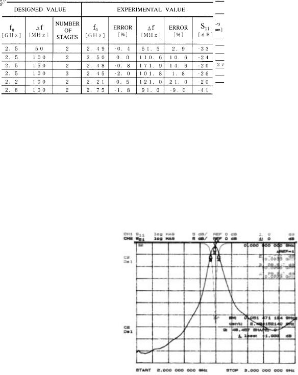
TABLE I
STRIP WIDTH Wi AND RESONATOR SECTION LENGTH Lj FOR VARIOUS BPF CHARACTERISTICS
WITH a = 5 mm, b = 3 mm, AND "c = 83
TABLE II
DESIGNED VALUES OF BPF CHARACTERISTICS AND EXPERIMENTAL VALUES
WITH a = 5 mm, b = 3 mm, AND "c = 83
broken line.  can be obtained by calculating


 in (33) and referring to Fig. 6. It must be noted that
  values depend on
  through (34) and (35).
 can be determined by (32).
We have designed a two-stage Butterworth BPF with


 GHz and bandwidth


 MHz. Metallic strip patterns are formed on the open surface of a DEW with width

 mm, height

 mm, and relative permittivity


 . The strip width
  and resonator section length
 are as follows:
 mm
mm


 mm
mm
 mm.
mm.
Fig. 7 shows the transmission and reflection characteristics of the experimental filter. After confirming a considerable agreement between the design and experimental results, we have designed and fabricated various BPF's. The designed values of BPF's characteristics and the dimension of strip patterns are shown in Table I, and the experimental values are shown in Table II. The center frequencies of the fabricated BPF's agree well with the prediction. Some fabricated BPF's have bandwidths equal to the designed values, and others have bandwidths considerably different from the design. The disagreement can be seen especially in the wide-band types and a low center-frequency type. These types of filters have short strip sections, which cause strong coupling between
Fig. 7. Transmission and reflection characteristics of fabricated filter with f0 = 2:5 GHz, bandwidth 1f = 50 MHz, a = 5 mm, b = 3 mm, "c = 83.
resonators. In the strong coupling region, it can be concluded that the theory is in error.
Finally, we touch on the open surface. Besides conductor loss and dielectric loss, there is radiation loss, which has not been analytically evaluated. The conductors more than 2 cm

1090 |
IEEE TRANSACTIONS ON MICROWAVE THEORY AND TECHNIQUES, VOL. 46, NO. 8, AUGUST 1998 |
apart from the open surface does not affect the characteristics of filters.
IV. CONCLUSION
Dielectric  -plane waveguides have been analyzed with full consideration of the outside field distribution, and the dispersion relation has been presented. Close agreement between calculated and experimental values was obtained. We have also calculated the coupling coefficients of
  -plane strips of the waveguide with assumed electric walls. Using these results, BPF's have been designed and fabricated. The center frequencies of the fabricated BPF's agree well with the designed values. Though the experimental bandwidth values are improved to some extent, compared with the previous results [4], the errors are still not small in the cases of wide bandwidths and low center frequencies. It should also be added that all the numerical analyses in this paper do not require a large-scale computer and can easily be carried out on a personal computer.
[8]R. F. Harrington, Time-Harmonic Electromagnetic Fields. New York: McGraw-Hill, 1961, ch. 8.
[9]Y. Konishi and K. Uenakada, ªThe design of a bandpass filter with inductive strip-planar circuit mounted in waveguide,º IEEE Trans. Microwave Theory Tech., vol. MTT-22, pp. 869±873, Oct. 1974.
[10]Y. C. Shih, ªDesign of waveguide E-Plane filters with all-metal inserts,º
IEEE Trans. Microwave Theory Tech., vol. MTT-32, pp. 695±704, July 1984.
Hiroshi Kubo (M'92) received the B.E., M.E., and D.E. degrees from Kyushu University, Fukuoka, Japan, in 1978, 1980, and 1993, respectively.
From 1980 to 1985, he was with the Nippon Electric Company, Tokyo, Japan, where he was engaged in development on mobile communication system. From 1985 to 1987, he worked as a Development Engineer at the Kyushu Matsushita Electric Company, Fukuoka, Japan. From 1987 to 1991, he was a Research Associate at Kyushu University. Since 1991, he has been with Yamaguchi University,
Ube-shi, Japan, where he is currently an Associate Professor. His main area of research interest is dielectric waveguides and waveguide components.
ACKNOWLEDGMENT
The authors thank R. Kitou and S. Furuya of Ube Industries, Ltd., Ube-shi, Japan, for providing them with the ceramic materials and Prof. M. Hano and A. Kirihara of Yamaguchi University, Ube-shi, Japan, for their helpful advice.
REFERENCES
[1]T. Nishikawa, ªFront end circuit components miniaturized using dielectric resonators for cellular portable telephones,º IEICE Trans., vol. E74, pp. 1556±1562, June 1991.
[2]M. Hano, S. Furuya, and I. Awai, ªThree-dimensional finite element analysis of dielectric E-plane waveguide filters,º in Proc. APMC'92, Adelaide, Australia, Aug. 1992, pp. 441±444.
[3]Y. Konishi, K. Konno, and I. Awai, ªNovel dielectric-waveguide components,º IEEE Trans. Broadcast., vol. 34, pp. 2±8, Mar. 1988.
[4]H. Kubo, I. Awai, K. Yamaguchi, and M. Hano, ªDesign and fabrication of bandpass filters based on a dielectric E-plane waveguide,º in IEEE MTT-S Int. Microwave Symp. Dig., vol. 1, San Diego, CA, May 23±27, 1994, pp. 241±244.
[5]R. E. Collin, Field Theory of Guided Waves. New York: McGraw-Hill, 1960, ch. 8.
[6]K. Yasuura, ªA view of numerical methods in diffraction problems,º in
Progress in Radio Science 1966±1969, W. V. Tilson and M. Sauzade, Eds. Brussels, Belgium: URSI, 1971, pp. 257±270.
[7]H. Kubo and K. Yasumoto, ªNumerical analysis of cylindrical dielectric waveguide with periodically varying radius,º IEICE Trans. Electron., vol. E74-C, pp. 384±390, Feb. 1991.
Hiroshi Yamashita (A'85) received the B. Eng. degree from Yamaguchi University, Ube-shi, Japan, in 1995.
Since 1995, he has been with the Kansai Heat Chemical Company, Kakogawa, Japan.
Ikuo Awai (M'78) received the B.S., M.S., and the Ph.D. degrees from Kyoto University, Kyoto, Japan, in 1963, 1965, and 1978, respectively.
In 1968, he joined the Department of Electronics, Kyoto University, as a Research Associate, where he was engaged in research on microwave magnetic waves and integrated optics. From 1984 to 1990, he worked for the Uniden Corporation, Tokyo, Japan, where he developed microwave communication equipments. In 1990, he joined Yamaguchi University, Ube-shi, Japan, where he is currently
a Professor. His research interests include the study of magnetostatic wave devices, dielectric waveguide components, and superconducting devices for microwave application.